 |
| Driver’s Side Fuse Box Diagram Of Hyundai Santa Fe 2010 |
Saturday, September 20, 2014
Driver’s Side Fuse Box Diagram Of Hyundai Santa Fe 2010
25W Class A Power Audio Amplifier Wiring diagram Schematic
This is the 25W Class-A power audio amplifier schema. The output devices are MJL4281A (NPN) and MJL4302A (PNP), and have high bandwidth, fantastic SOA (safe operating area), high linearity and high gain. Driver transistors are MJE15034 (NPN) and MJE15035 (PNP). All devices are rated at 350V, using the power transistors having a 230W dissipation and the drivers are 50W.
25W Class-A Power Audio Amplifier Circuit Diagram
- The supply voltage must be a maximum of ±25V. This supply is simply obtained from a 20-0-20V transformer, recommended current is 1A.
- All resistors ought to be 1/4W or 1/2W 1% metal film for lowest noise, with the exception of R9, R10 and R15 which ought to be 1/2W varieties, and R13, R14 have to be 5W wirewound.
- Using the suggested and advised 25V supplies, Q4 will typically not need a heatsink. The output drivers (Q5 and Q6) recommended to use a heatsink, even though it doesn’t have to be big.
Fuse Box F250 2008 Ford Superduty 4WD Diagram
Fuse Box F250 2008 Ford Superduty 4WD Diagram - Here are new post for Fuse Box F250 2008 Ford Superduty 4WD Diagram.


Fuse Panel Layout Diagram Parts: blower motor relay, low to hi relay, heated mirror, A/C clutch relay, PCM power relay, starter relay, trailer tow relay, park lamp, trailer tow relay battery charger, run start relay, fuel pump motor diode, A/C clutch diode, stoplamp, trailer tow relay, reversing lamp relay, fuel pump relay.
Fuse Box F250 2008 Ford Superduty 4WD Diagram


Fuse Panel Layout Diagram Parts: blower motor relay, low to hi relay, heated mirror, A/C clutch relay, PCM power relay, starter relay, trailer tow relay, park lamp, trailer tow relay battery charger, run start relay, fuel pump motor diode, A/C clutch diode, stoplamp, trailer tow relay, reversing lamp relay, fuel pump relay.
Friday, September 19, 2014
TDA2040 20W HI FI Audio Amplifier
Here the hi-fi power amplifier schema which will deliver 20W power output. This amplifier schema use single power IC TDA2040 and a few external components.

Detailed explanation about this 20W Power Amplifier
Fuse Box Ford 2006 SUV Diagram
Fuse Box Ford 2006 SUV Diagram - Here are new post for Fuse Box Ford 2006 SUV Diagram.

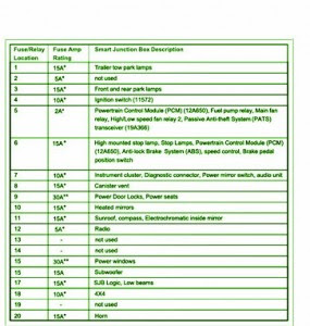
Fuse Panel Layout Diagram Parts: trailer tow park lamp, park lamp, ignition switch, powertrain control module, fuel pump relay, main fan relay, passive anti theft system, high mounnted stop lamp, stop lamp, powertrain control module, brake pedal position switch, instrument cluster, diagnostic connector, power mirror switch, audio unit, canister vant, power seats, sunroof, compass, radio, power window, suwoofer, low eams, horn.
Fuse Box Ford 2006 SUV Diagram


Fuse Panel Layout Diagram Parts: trailer tow park lamp, park lamp, ignition switch, powertrain control module, fuel pump relay, main fan relay, passive anti theft system, high mounnted stop lamp, stop lamp, powertrain control module, brake pedal position switch, instrument cluster, diagnostic connector, power mirror switch, audio unit, canister vant, power seats, sunroof, compass, radio, power window, suwoofer, low eams, horn.
Simple Video Amplifier
The video amplifier in the diagram is a well-known design. Simple, yet very useful, were it not for the ease with which the transistors can be damaged if the potentiometers (black level and signal amplitude) are in their extreme position. Fortunately, this can be obviated by the addition of two resistors.
Circuit diagram :
 Simple Video Amplifier Circuit Diagram
If in the diagram R 3 and R 4 were direct connections, as in the original design, and P 1 were fully clockwise and P 2 fully anticlockwise, such a large base current would flow through T 1 that this transistor would give up the ghost. Moreover, with the wiper of P 2 at earth level, the base current of T 2 would be dangerously high. Resistors R 3 and R 4 are sufficient protection against such mishaps, since they limit the base currents to a level of not more than 5 mA.
Shunt capacitor C 4 prevents R 4 having an adverse effect on the amplification.
Automatic Night Light Feeds Directly From the AC Line
There are many approaches to the problem of activating a light when it becomes dark, and a recent Design Idea covers this topic (Reference 1). Some approaches require a dc power supply and an electromechanical relay, but a better approach involves feeding the device directly from the ac line, minimizing the number of components
(Figure 1).

Figure 1. The photoresistor activates the TRIAC and the load when darkness falls.
The heart of the device is a light-sensitive cadmium-sulphide resistor, PR, with a resistance of approximately 200 kΩ in the dark and decreasing to a few kilohms in the light. PR and capacitor C1 form an ac-voltage divider. In daylight, the voltage across PR is too low to generate the required gate-trigger current to turn on bidirectional ac switch Q1, thus keeping the load – usually a lamp – off. When it becomes dark, PR’s resistance rises, resulting in an increase in the TRIAC’s gate current that triggers the TRIAC and lights the lamp.
The schema uses inexpensive, off-the-shelf components, including the VT90N1 photoresistor; a 0.1-μF, 275V capacitor; and an L2004F61 TRIAC with a load current of 4A rms, a peak blocking voltage of 200V, and a gate-trigger current of 5 mA. The exact specifications of these components are not critical; you could use others instead.
Editor’s note:
Attributes worth mentioning include the fact that the capacitor introduces a phase shift, which places the peak of the gate voltage close to the zero crossing of the load’s sine wave for optimum turn-on timing. Another benefit is thermal hysteresis, which occurs due to the reduction of the required triggering voltage and current as the TRIAC warms up after the initial turn-on.
Thursday, September 18, 2014
4 x 12 W power amplifier with dynamic distortion detector and diagnostic interface
FEATURES
Requires very few external components
High output power
Fixed gain
Diagnostic facility (distortion, short-circuit and temperature detection)
Good ripple rejection
Mode select switch (operating, mute and stand-by)
Load dump protection
AC and DC short-circuit safe to ground and to VP
Low power dissipation in any short-circuit condition
Thermally protected
Reverse polarity safe
Electrostatic discharge protection
No switch-on/switch-off plop
Flexible leads
Low thermal resistance
Identical inputs.
GENERAL DESCRIPTION
The TDA8562Q is an integrated class-B output amplifier in a 17-lead single-in-line (SIL) power package. It contains 4 × 12 W single-ended amplifiers.
Circuit Diagram
 |
| 4 x 12 W power amplifier with dynamic distortion detector and diagnostic interface |
Fuse Box Ford 1989 Ranger Two Wheel Drive Diagram
Fuse Box Ford 1989 Ranger Two Wheel Drive Diagram - Here are new diagram for Fuse Box Ford 1989 Ranger Two Wheel Drive Diagram.

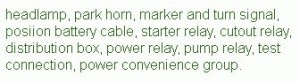
Fuse Panel Layout Diagram Parts: headlamp, park horn, marker and turn signal, posiion battery cable, starter relay, cutout relay, distribution box, power relay, pump relay, test connection, power convenience group.
Fuse Box Ford 1989 Ranger Two Wheel Drive Diagram


Fuse Panel Layout Diagram Parts: headlamp, park horn, marker and turn signal, posiion battery cable, starter relay, cutout relay, distribution box, power relay, pump relay, test connection, power convenience group.
5V Power Supply Using LTM8021
This 5v power supply circuit is designed using the LTM8021 and will provide a maximum current up to 500mA. Almost all required parts are included in the LTM8021 package. This 5v power supply circuit based on the LTM8021 operate over a input voltage range between 3V and 36V .The LTM8021 supports an output voltage range of 0.8V to 5V, set by a single resistor. Only an output and bulk input capacitor are needed to finish the design.
5V Power Supply Circuit diagram

5V Power Supply Circuit diagram
Wednesday, September 17, 2014
SONY KLV 32S550A KLV 26S550A – HOW TO DISASSEMBLE – LED BLINKING CODES

SONY KLV-32S550A - KLV-26S550A –DISASSEMBLE – LED BLINKING CODES
KLV-32S550A (RM-GA016) – [GE, ME, Philippines, (Blue) Russia, South Africa]
KLV-32S550A/T (RM-GA016) [GE, ME, Philippines, (Brown) Russia, South Africa]
KLV-37S550A (RM-GA016) [GE, India, Iran, ME, Philippines, Russia, Thailand, Tunisia]
LED BLINKING CODES – SELF DIAGNOSIS FUNTION – REMOVAL OF BACK COVER & SCREW SIZES.
Blinking codes: Triangle chart
KLV-26S550A, 32S530A, 32S550A, 32S550A/L, 32S550A/T
KLV-37S550A
R2 Board and Rear Cover Removal. [KLV-26S550A/1, 26S550A/3]
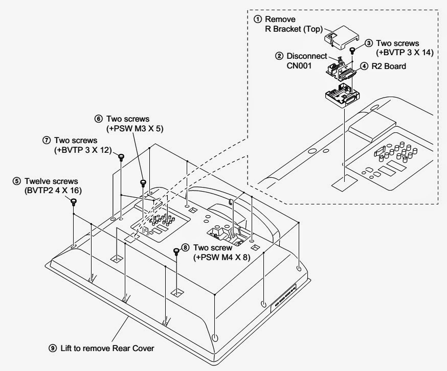
R2 and Rear Cover Removal [KLV-32S550A/1, 32S550A/3]

Removal of Rear Cover Procedure
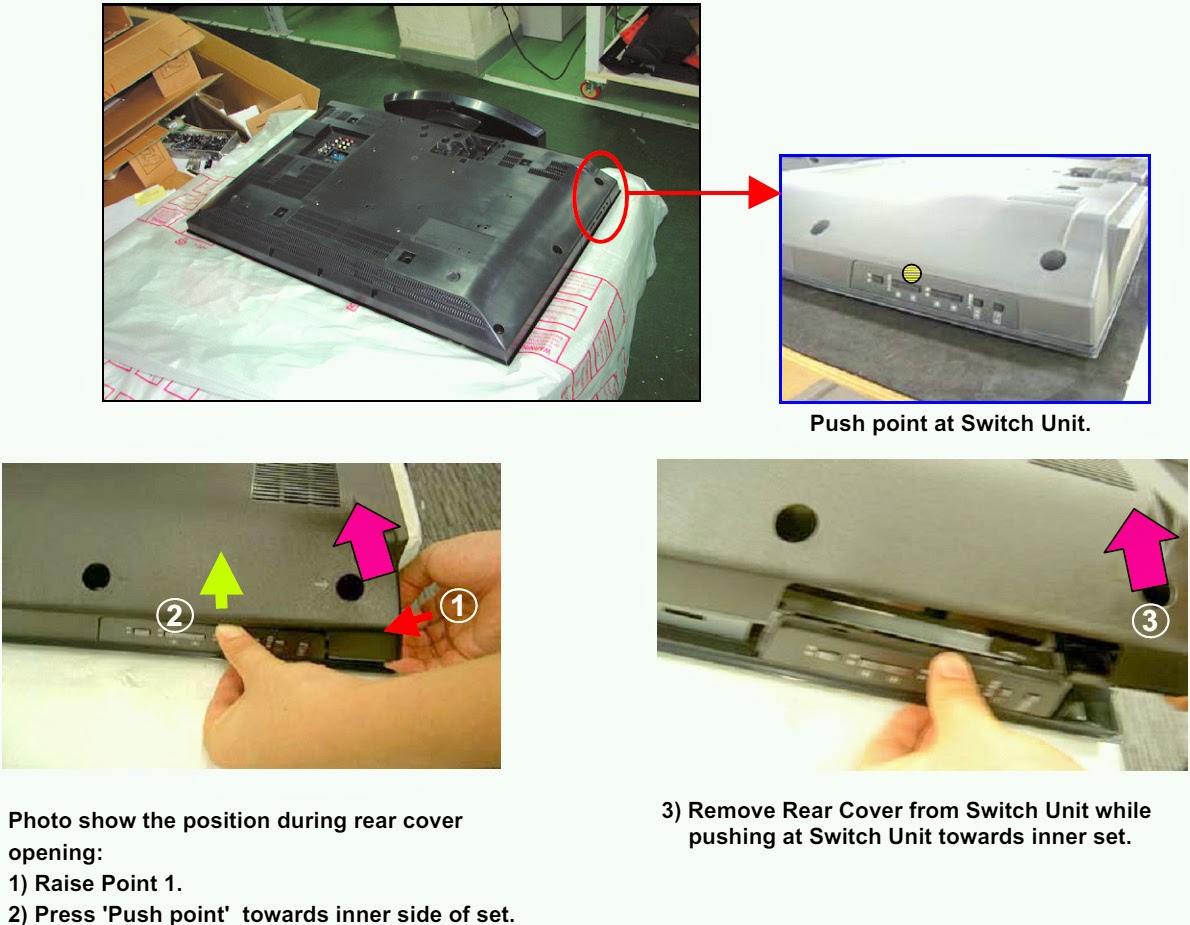
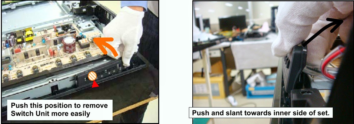
Removal of Switch Unit
Push and slant towards inner side of set to remove Switch Unit correctly.
Fuse Box BMW Cibie CSR Diagram
Fuse Box BMW Cibie CSR Diagram - Here are new post for Fuse Box BMW Cibie CSR Diagram.


Fuse Panel Layout Diagram Parts: high beam relay, low beam relay, auxiliary fan, turn signal, windshield wiper/washer, intensive cleaner, brake light, cruise control, horn, engine electrical equipment, back up light, fuel pump, check control, instrument cluster, on board computer, heater blower, back up light, outside power mirror, mirror heating, air conditioner, power seat memory, rear window defogger, interior light, glove box, memory, rechargable flash light, hazard warning light, engine compartment light, license plate light, power antenna, parked car heater, fog light.
Fuse Box BMW Cibie CSR Diagram
Fuse Panel Layout Diagram Parts: high beam relay, low beam relay, auxiliary fan, turn signal, windshield wiper/washer, intensive cleaner, brake light, cruise control, horn, engine electrical equipment, back up light, fuel pump, check control, instrument cluster, on board computer, heater blower, back up light, outside power mirror, mirror heating, air conditioner, power seat memory, rear window defogger, interior light, glove box, memory, rechargable flash light, hazard warning light, engine compartment light, license plate light, power antenna, parked car heater, fog light.
Tuesday, September 16, 2014
Fuse Box Ford 2005 Freestyle Diagram


Fuse Box BMW R1150GS Diagram
Fuse Box BMW R1150GS Diagram - Here are new post for Fuse Box BMW R1150GS Diagram.
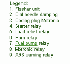
Fuse Panel Layout Diagram Parts: flasher unit, dial needle damping, coding plug motronic, starter relay, load relief relay, horn relay, fuel pump relay, motronic relay, ABS warning system.
Fuse Box BMW R1150GS Diagram
Fuse Panel Layout Diagram Parts: flasher unit, dial needle damping, coding plug motronic, starter relay, load relief relay, horn relay, fuel pump relay, motronic relay, ABS warning system.
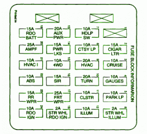
Explanation Fuse Box Chevy s10 2001 Diagram
Fuse Box Chevy s10 2001 Diagram - This show you about Fuse Box Chevy s10 2001 Diagram.


Fuse Panel Layout Diagram Parts: back up lamp, supply voltage, trailer rear, stop lamp supply, back lamp supply, park lamps supply voltage, trailer CHMSL supply voltage, fuel pump supply, ignition voltage.
Fuse Box Chevy s10 2001 Diagram
Fuse Panel Layout Diagram Parts: back up lamp, supply voltage, trailer rear, stop lamp supply, back lamp supply, park lamps supply voltage, trailer CHMSL supply voltage, fuel pump supply, ignition voltage.
Monday, September 15, 2014
Noise Suppression For R C Receivers
Receiver interference is hardly an unknown problem among model builders. Preventive measures in the form of ferrite beads fitted to servo cables are often seen in relatively large models and/or electrically driven models, to prevent the cables from acting as antennas and radiating interference to the receiver. If miniature ferrite beads are used for this purpose, the connector must be first be taken apart, after which the lead must be threaded through the bead (perhaps making several turns around the core) and then soldered back onto the connector. An interference source can also cause problems in the receiver via the power supply connection.

The battery is normally connected directly to the receiver, with the servos in turn being powered from the receiver. The servos can draw high currents when they operate, which means they can create a lot of noise on the supply line. This sort of interference can be kept under control by isolating the supply voltage for the receiver from the supply voltage for the servos. All of these measures can easily be implemented ‘loose’ in the model, but it’s a lot nicer to fit everything onto a single small schema board. That makes everything look a lot tidier, and it takes up less space.

The schematic diagram is shown in Figure 1. Connectors K1–K8 are located at the left. They are the inputs for the servo signals, which are connected to the receiver by the servo leads. The outputs (K9–K16) are located on the right. That is where the servos are connected. Finally, the battery is connected to K17. Interference on the supply voltage line due to the motors and servos is suppressed by a filter formed by L10, R1, C1 and C2. L10 is a ferrite-core coil with an impedance of 2000 ohms at 30 MHz. In combination with C1 and C2, it forms a substantial barrier to interference in the 35-MHz R/C band.

Signals with frequencies close to the 10.4-MHz intermediate frequency (which is used in many receivers) are also effectively blocked by this filter. L9 filters out common-mode noise on the supply line for the servos, which effectively means that it prevents the supply lines to the servos from acting as antennas. Finally, high-frequency currents on the servo signals are filtered out by ferrite beads in order to limit the antenna effects of these connection lines.
Resistor:
- R1 = 1Ω
- C1 = 100nF
- C2 = 22pF
- L1-L8,L10 = ferrite inductor
- L9 = common-mode coil
- K1-K8 = servo cable
- K9-K17 = 3-way SIL pinheader
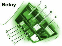
Mercedes Explanation Fuse Box Year Benz 1995 C280 Diagram
Fuse Box Mercedes Benz 1995 C280 Diagram - Below is Fuse Box Mercedes Benz 1995 C280 Diagram.
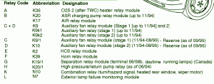
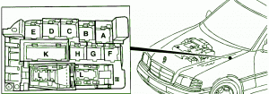
Fuse Panel Layout Diagram Parts: heater relay module, ASR charging pump relay module, A/R relay module, auxiliary relay fan module, HCS realay module, horn relay module, daytime running lamp, return pump relay, combination relay, hazard signal, heated rear window, wiper motor, exterior lamp failure monitoring module.
Fuse Box Mercedes Benz 1995 C280 Diagram
Fuse Panel Layout Diagram Parts: heater relay module, ASR charging pump relay module, A/R relay module, auxiliary relay fan module, HCS realay module, horn relay module, daytime running lamp, return pump relay, combination relay, hazard signal, heated rear window, wiper motor, exterior lamp failure monitoring module.
Relay Based Motorcycle Alarm Wiring diagram Schematics
You can Make Relay Based Motorcycle Alarm Circuit Diagrams. You can use them to protect your motorcycle - but they have many more applications. If you use relays with 6-volt coils - theyll protect your "Classic Bike". Both alarms are very small. The completed boards occupy about half a cubic-inch - 8 cc. The standby current is zero - so they wont drain your battery.
Relay Based Motorcycle Alarm Circuit Diagram 1 uses a SPCO/SPDT relay - but you really only need to use a SPST relay. If you are going to use the veroboard layout provided - youll need to use the style of relay specified. But you can build the alarm using whatever style of relay you have available.
Relay Based Motorcycle Alarm Circuit Diagram 1

Any number of normally-open switches may be used. Fit the mercury switches so that they close when the steering is moved or when the bike is lifted off its side-stand or pushed forward off its centre-stand. Use micro-switches to protect removable panels and the lids of panniers etc. When one of the trigger-switches is closed - the relay will energize and the siren will sound.
You can choose what happens next. If you build the schema as shown, the siren will continue to sound until you turn it off - or until the battery is exhausted. But, if you leave out D3 - the siren will stop sounding immediately the trigger-switch is re-opened.
While youre within earshot of your machine - the former configuration is best. You can always turn off the alarm yourself. But if you are going to be away from your bike for any length of time - and you dont want to cause a nuisance - then the latter configuration is probably more suitable. If you include a SPST switch in series with D3 - you can select the behaviour that best suits the circumstances at any given time.
Relay Based Motorcycle Alarm Circuit Diagram 1a
Relay coils and some sounders produce high reverse-voltage spikes that will destroy sensitive electronic components. D1 and D2 are there to short-schema these spikes before they can do any damage. Although there is nothing in the alarm schema itself that could be damaged - I have no idea what other electronic equipment might be connected to the same power supply. So I included the two diodes as a precaution. If youre satisfied that theres nothing on your bike that might be damaged in this way - you can leave out the two diodes.
Relay Based Motorcycle Alarm Circuit Diagram 2 uses a DPCO/DPDT relay - but you really only need to use a DPST relay. If you are going to use the veroboard layout provided - youll need to use the style of relay specified. But you can build the alarm using whatever style of relay you have available.
Relay Based Motorcycle Alarm Circuit Diagram 2
Any number of normally-open switches may be used. Fit the mercury switches so that they close when the steering is moved or when the bike is lifted off its side-stand or pushed forward off its centre-stand. Use micro-switches to protect removable panels and the lids of panniers etc. When one of the trigger-switches is closed - the relay will energize and the siren will sound.
You can choose what happens next. If you build the schema as shown, the siren will continue to sound until you turn it off - or until the battery is exhausted. But, if you leave out the (yellow) solder-bridge in the top left-hand corner of the diagram - the siren will stop sounding immediately the trigger-switch is re-opened.
While youre within earshot of your machine - the former configuration is best. You can always turn off the alarm yourself. But if you are going to be away from your bike for any length of time - and you dont want to cause a nuisance - then the latter configuration is probably more suitable. Connect a SPST switch in place of the (yellow) solder-bridge - and you can select the behaviour that best suits the circumstances at any given time.
Relay Based Motorcycle Alarm Circuit Diagram 2 a
Relay coils and some sounders produce high reverse-voltage spikes that will destroy sensitive electronic components. D1 and D2 are there to short-schema these spikes before they can do any damage. Although there is nothing in the alarm schema itself that could be damaged - I have no idea what other electronic equipment might be connected to the same power supply. So I included the two diodes as a precaution. If youre satisfied that theres nothing on your bike that might be damaged in this way - you can leave out the two diodes.
Whichever alarm you build - the schema board and switches must be protected from the elements. Dampness or condensation will cause damage. Without the terminal blocks - the board is small. Ideally, you should try to find a siren with enough spare space inside to accommodate it. Fit a 1-amp in-line fuse as close as possible to the power source. This is Very Important. The fuse is there to protect the wiring - not the schema board. Instead of using a key-switch you can use a hidden switch; or you could use the normally-closed contacts of a small relay. Wire the relay coil so that its energized while the ignition is on. Then every time you turn the ignition off - the alarm will set itself.
When the alarms are not sounding - the diagram use no current. This should make them useful in other circumstances - where a power supply is not readily available. Powered by dry batteries - with the relay and siren voltages chosen to suit - the alarms could be fitted almost anywhere.
Sourced By : Streampowers
Sunday, September 14, 2014
Explanation Fuse Box Chevrolet ZR2 2003 Diagram
Fuse Box Chevrolet ZR2 2003 Diagram - This show you about Fuse Box Chevrolet ZR2 2003 Diagram.

Fuse Panel Layout Diagram Parts: cigar lighter, data link connector, body control module, cruise control module, multifunction switch, driver front passenger, instrument panel cluster, view mirror switch, door lock, side window lock out switch, audio control, IP ashtray lamp, redundant steering wheel control, headlamp switch, seat lumbar switch,
Fuse Box Chevrolet ZR2 2003 Diagram
Fuse Panel Layout Diagram Parts: cigar lighter, data link connector, body control module, cruise control module, multifunction switch, driver front passenger, instrument panel cluster, view mirror switch, door lock, side window lock out switch, audio control, IP ashtray lamp, redundant steering wheel control, headlamp switch, seat lumbar switch,
SW Converter for Digital AM Car Radio
SW Converter for Digital AM Car Radio Circuit Diagram This schema is purposely presented with many loose ends (not literally, of course) to stimulate experimenting with RF schemary at a small outlay. Looking at the schema diagram you may recognize a modified version of the SW Converter for AM Radios described elsewhere in this issue. The modifications were necessary to make the schema compatible with a digital rather than analogue AM car radio. The main difference between digital AM radios and their all-analogue predecessors is that tuning is in 9 kHz (some-times 4.5 kHz steps) in compliance with the international frequency allocation for the band. Obviously, that particular step size, desirable as it may be on MW, is a stumbling block if you want to use a digital AM receiver in combination with a frequency step-up converter for SW, where chaos reigns and there is no fixed step size. The first attempt was to make the crystal oscillator variable by about 5 kHz each way.
SW Converter for Digital AM Car Radio Circuit diagram :
SW Converter for Digital AM Car Radio Circuit Diagram
Unfortunately, despite serious efforts, the crystal could not be pulled more than 1 or 2 kHz so another solution had to be found. After studying the NE/SA602/612 datasheet, it was found that a variable LC based oscillator was the best alternative. The schema worked after winding a resonant LC schema and adding a 0.1 µF series capacitor to block the DC component on pin 6 of the NE602 (612). When the tuning was found to be a bit sharp with the original capacitor, a simple bandspread (or fine tuning) feature was added by shunting the LC resonant schema with a lightly loaded 365 pF tuning capacitor (C10) which, like the main tuning counterpart, C8, was ratted from an old transistor radio. The tuning coil, L1, consists of 8 to 10 turns of 0.6-0.8mm dia. enamelled copper wire (ECW) on a 6-8 mm dia. former without a core. With this coil, frequency coverage will be from about 4 MHz to 12 MHz or so. Details on Tr1 may be found in the referring article.
Note that no tuning capacitor is used on the secondary — the input stray capacitance of the NE602 (612) does the trick. A BFO (beat frequency oscillator) was added to enable SSB (single sideband) signals to be received. The BFO built around T1 is simple, has a heap of output and is stable enough to hold an SSB signal for a few minutes without adjustment. The BFO frequency is tuned with C3. Tr2 is a ready-made 455 kHz IF transformer whose internal capacitor was first crushed and then removed with pliers. When S2 is closed the BFO output signal is simply superimposed on the NE602 (612) IF output to the MW radio. The converter should be built into a metal box for shielding. If you find that the BFO gives too much output, disconnect it as suggested in the schema diagram and let stray coupling do the work. Sensitivity, even on a 1-metre length of car radio aerial, is quite amazing. Bearing in mind that most of the major international SW broadcasting stations like Radio NHK Japan, Moscow, BBC etc.) generate enough power to make sure that you will hear them, it is still quite exciting to hear such signals for the first time on your car radio.
20W Bridge Audio Amplifier Wiring diagram Schematic
Specifications:
- 20W Bridge Audio Amplifier kit, based on the TDA2005 IC, a class B dual audio amplifier, specifically designed for car radio applications etc.
- Power supply - 18 VDC
- Output power - 20 W, 4 Ω
- IC built in Thermal Shut-down, Load dump voltage surge protected
- Terminal pins for connecting left and right audio signal inputs
- Relimate Connector for connecting Potentiometer (POT) for volume adjustment
- Power Battery Terminal (PBT) for easy power supply and speaker connection
- Power-On LED indicator
- Heatsink for IC
- Four mounting holes of 3.2 mm each with nut and stud
- PCB dimensions 63 mm x 65 mm
20W Bridge Audio Amplifier Circuit Diagram
Pcb

Parts List

Saturday, September 13, 2014
Samsung will introduce the Galaxy Note 4 on 3 September
It is expected that Samsung present its new phone Samsung Galaxy Note 4 officially in September during IFA 2014 event held in Berlin, Germany. Now, the Korean media already have an exact date of this phone Samsung.
According to The Korea Times, Samsung will be announcing the Galaxy Note 4 on September 3, a day before the presentation of the Galaxy Note 3 last year.
Samsung is expected to start sending invitations to the event "soon", including that the company would be a bit rushed to launch its new mobile big Lcd because Apple is finally breaking its tradition of offering only one size cell relatively small as the iPhone 6 to gain entry to the high-end market. It is said that Samsung is trying to get the Galaxy Note sale 4 days before what went on Galaxy Note 3 with this same purpose.
It is expected that the Samsung Galaxy Note 4 has a QHD (2560 × 1440) 5.7 inch Lcd, a Snapdragon 805 / Exynos 5433 processor, 3GB of RAM and a 16 megapixel camera that would include the Sony IMX240 sensor. Additionally, he said that the Samsung Galaxy Note 4 would an ultraviolet sensor and Android KitKat.
Wheatstone bridge
A Wheatstone bridge is an electrical schema used to
measure an unknown electrical resistance by balancing two
legs of a bridge schema, one leg of which includes the
unknown component. Its operation is similar to the original
potentiometer. It was invented by Samuel Hunter Christie in
1833 and improved and popularized by Sir Charles
Wheatstone in 1843. One of the Wheatstone bridges initial
uses was for the purpose of soils analysis and
comparison.
Operation
In the figure, is the unknown resistance to be measured; , and are resistors of known resistance and
the resistance of is adjustable. If the ratio of the two resistances in the known leg is equal to the ratio of
the two in the unknown leg , then the voltage between the two midpoints (B and D) will be zero and no
current will flow through the galvanometer . If the bridge is unbalanced, the direction of the current indicates
whether is too high or too low. is varied until there is no current through the galvanometer, which then reads
zero.
Detecting zero current with a galvanometer can be done to extremely high accuracy. Therefore, if , and
are known to high precision, then can be measured to high precision. Very small changes in disrupt the
balance and are readily detected.
At the point of balance, the ratio of
12 Watt Audio Amplifier

This low cost amplifier is simple and give you good result. Here the op-amp used is uA 741 which produces the required gain.The four transistors are wired as complementary Darlington’s which produces the drive for the speaker.
The voltage drop across the resistors R2 and R3, are used as the input of the Darlington pairs . As the input current to the op-amp depends on the level of the signal op amp is amplifying the voltage drop across the resistors R2 and R3 will be proportional to the input signal. These voltage drops are given to the base of Darlington pairs. The amplification is stabilized as a result of the negative feedback from the junction of collectors of Q2 and Q4. The theory may seem little awkward for you. But its working good.cSuch a simple but stable schema as this can produce a reasonable output of 12W on a 4 Ohm speaker.
Friday, September 12, 2014
10 to 14W Class A Audio Amplifier Wiring diagram Schematic
I have built this amplifier and it does sound good. It requires a preamp as it hasnt got much gain. It requires big heat sinks and a large transformer and a great power supply and careful wiring, but in the end it is xtremely simple and it sounds very good. The zener diode rejects any ripple coming from the power supply, But you still only want a ripple of 10mV max. The ripple reaching the input is amplified, so the zener diode gets rid of that, but whatever ripple there is will still reach the power stage.
Simple Portable Solar Lantern Wiring diagram Schematic
This is the Simple Portable Solar Lantern Circuit Diagram. This portable solar lantern schema uses 6 volt/5 watt solar panels are now widely available. With the help of such a photo-voltaic panel we can construct an economical, simple but efficient and truly portable solar lantern unit. Next important component required is a high power (1watt) white LED module.
Simple Portable Solar Lantern Circuit Diagram
When solar panel is well exposed to sunlight, about 9 volt dc available from the panel can be used to recharge a 4.8 volt /600 mAh rated Ni-Cd batterypack. Here red LED (D2) functions as a charging process indicator with the help of resistor R1. Resistor R2 regulates the charging current flow to near 150mA.
Assuming a 4-5 hour sunlit day, the solar panel (150mA current set by the charge controller resistor R2) will pump about 600 – 750 mAh into the battery pack. When power switch S1 is turned on, dc supply from the Ni-Cd battery pack is extended to the white LED (D3). Resistor R3 determines the LED current. Capacitor C1 works as a buffer.
Note: After construction, slightly change the values of R1,R2 and R3 up/down by trial&error method, if necessary.
DC to AC with NE 555
This is a inverter schema by using this schema you can get 230v current.If your an under age one be careful when you deal with this.Always try to get the assistance of an elder.If there was a fault we cant get the responsibility of it.


