Thursday, November 20, 2014

8 Relay Control Circuit

8 Relay Control Circuit
R1-8=4.7 Kohms T1-8= BD139 (R1-8=15 Kohms if T1-8=BD679)
RL1-8=6V-24V dc Relay D1-8=1N4148
8 

Crystal Radio Audio Amplifier Circuit

CrystalCrystal Radio Audio Amplifier Circuit

Here is a simple audio amplifier application a TL431 blow regulator. The amplifier will accommodate room-filling aggregate from an accustomed clear radio outfitted with a long-wire antenna and acceptable ground. The chip is agnate in complication to a simple one-transistor radio but the achievement is far superior.

The TL431 is accessible in a TO-92 amalgamation and it looks like an accustomed transistor so your hobbyist accompany will be afflicted by the aggregate you are accepting with alone one transistor! The amplifier may be acclimated for added projects, too. Higher impedance headphones and speakers may additionally be used. An earphone from an old blast will accord boisterous aggregate and abundant sensitivity! The 68 ohm resistor may be added to several hundred ohms back application aerial impedance earphones to save array power.

Wednesday, November 19, 2014

Toggle Switch with IR

Toggle switch in this article is a series of toggle switches that are controlled by infrared light. The series toggle switch is made from a combination of data flip-flop CD4013 2 units. Receiver circuit of the infrared light signals arranged with infrared receiver as found on television remote receiver. Infrared signal from remote is used as clock signals and data to the data flip-flop first. then the second flip-flop data set as a toggle flip-flop toggle the output signal is used to drive the relay. for more details can be seen in thethe following image .


Toggle


Series Toggle Switch With Infra Red (IR) that is required to supply voltage range of 12VDC and the output of Toggle Switch With Infra Red (IR) is dapt used to turn on the lights or other electronic devices with DC or AC voltage source. Series Toggle Switch With Infra Red (IR) was isolated from the load that is placed for use as the final relay.

Variable Speed ​​DC Motor Controller 12V

For more details can be seen from a series of Variable Speed ​​DC Motor Controller 12V follows.

Series Variable Speed ​​DC Motor Controller 12V This is one series that can be used to regulate speed DC12V motor with PWM technique. Series Variable Speed ​​DC Motor Controller 12V uses a 555 timer IC as a PWM pulse generator to regulate the motor speed DC12 Volt. DC motor speed control process performed by adjusting the potentiometer R1 lever which in principle is set High and Low pulse width of the PWM pulse.

Series Variable Speed ​​DC Motor Controller 12V above the power MOSFET drivers in the form of a IRFZ46N is directly associated with DC motors. Working voltage of this circuit can be adjusted according to needs-driven DC motor, this circuit can work from 3-18VDC.

Stereo Power Amplifier STA550

Stereo Power Amplifier 2x70Watt STA550 is chip audio power with BASH concept that can be connected with digital devices. 2x70Watt STA550 Stereo Power Amplifier is an amplifier with BTL system with symmetrical power supply with ground. Power amplifier STA550 uses power output transistor which is on the chip and is set to produce a high efficiency audio power. Power output on the STA550 is using the system without copling ac bridge (direct) and zero offset.

Strengthening of the STA550 from stereo power amplifier is +12 dB. 2x70Watt STA550 Stereo Power Amplifier is equipped with temperature sensors for protection from overheating and current-limiting protection system for power amplifier. 2x70Watt STA550 Stereo Power Amplifier is equipped with standby and mute controls to regulate silent or active mode power amplifier.


    Feature :

  •      Monochip Bridge Stereo Amplifier with Bash ® Architecture
  •      55 +55 w Output Power @ Rl = 4 / 8 W, THD = 0.5%
  •      70 +70 w Output Power @ Rl = 4 / 8 W, THD = 10%
  •      High Dynamic preamplifier Input Stages
  •      Programmable External Feedback Type Compressors
  •      AC Coupled Input Output Bridge To Class Ab Amplifier
  •     Precision Rectifiers To Drive The Digital Converter
  •      Proportional Over Power Output Current Limit To The Digital Converter
  •      Absolute Power Transistor Bridge Output Power Protection
  •      Absolute Output Current Limit
  •      Integrated Thermal Protection
  •      Power Supply Over-Voltage Protection Flexiwatt With 27 Pin Power Package
  •      Bash ® Licence Require

Tuesday, November 18, 2014

10Mhz to 1 MHz Frequency Converter

10Mhz to 1 MHz Frequency Converter Circuit

10Mhz

Part ListIC1 7404 = 1
IC2 7490A = 1
R 1 K = 2
R 3.3 K = 1
C Trim Polymer 39 pF = 1
C Electrophoresis 4.7 uF 16V = 1
C Milar 47 nF 16 V = 1
C Milar 10 nF 16 V = 1
C Ceramic 68 pF 50 V = 1 

Seven Segment 4 Digit

Seven segment 4 Digit display Multiplex in electronic device applications is drain port  a micro controller or data point that will be on display, especially if the data to be displayed more than 1 digit. necessary path to control the resources of each 7 segment and the path to input data on the 7 segment. Circuit 7 Segment 4 Digit Multiplex is a way to save the port or micro controller data path that will be displayed. Series Display 7 Segment 4 Digit Multiplex uses BCD to 7 segment decoder 74LS247 BCD to encode data from the data that will be displayed, then for each resource viewer 7 segment using the set of transistors as electronic switches. Current flowing in the viewer in a series of 7 segment Display 7 Segment 4 Digit Multiplex is in limiting use yag resistor in series pairs in each collector transistor.


Resistors are mounted in series of LED is used as a barrier for current flow that flows through the LED does not exceed the maximum allowable, current that is equal to 20 mA.

Make 5 1 Channel Audio Amplifier

5.1 channel amplifier consists of 6 amplifiers 1 channel mono, which has certain specifications on each canals. Has 6 channel surround sound amplifier that consists of Front Left ,Center,Front Right ,Rear Left (Left Surround),Rear Right (Right Surround) , and LFE (Subwoofer).For clarity I give a simple illustration of the layout and the circuit for these speakers.

5.1 Speaker Setup

Accoustic Field Generator
Acoustic Field Generator is generating acoustic sound with surround effects are adjustable with a standard Dolby Surround, able to produce surround sound is good enough but not too much need of funds. Technological developments as if not only focused on one area alone but on all fronts. The development of technologies that exist today one of them is in the field of audio. With more advanced audio technology today not only as mere entertainment but has become a hobby, hobby is not cheap of course. Many audio enthusiasts trying to make music sound that sounded to be very hard to make music sound as live, the addition of the amplifier, woofer or special speakers that cost is not cheap.

The sound effects are living seems to now is something that most do not have to exist in every good audio devices. This effect is basically a surround effect that can lead to sound as though coming from different directions and his voice can still be heard clearly. Currently Compo-tape tape that has been a lot of these facilities surround sound but not good enough when heard from a considerable distance because of the effects surroundnya missing. This is because the distance is too far listener and speaker, speaker layout is not quite right, or the effect of unfavorable surround.


Surround effects are nice and can be heard with a good surround system is a system that is in movie theaters and to make it not a bit prangkat needed funds. However, if satisfaction remains the number one then the fund is not a major problem. To find a middle ground between price and quality surround effects it was attempted to make the Acoustic Field Generator that can produce surround sound is good enough but not too much need of funds. Acoustic Field Generator is capable of generating acoustic sound with surround effects are adjustable with a standard Dolby Surround.


Accoustic Field Generator Construction

Basically an Acoustic Field Generator built from op-amp circuit and filters. Op-amps are usually used as a voltage amplifier in the Acoustic Field Generator is more widely used as active filters. The filter in the tool is very instrumental in creating an acoustic sound that is really clear, but in practice, almost all the filters, do not miss the precision of the signal with a specific frequency. An op-amp is good for this application is the op-amp which has a wide bandwidth, rise time, slew rate and fast setting timenya. In addition to op-amp and active filter, theres more important parts of the power supply. This is the part that is instrumental in creating excellence acoustic sound because of the bad power supply which is the only producer of noise, which will enter into a voice signal path so that should clear acoustic sound into an acoustic sound with the addition of reverberation (noise). The power supply used is the twin power supply + / - 18 volts DC. Part Acoustic Field Generators


Before we start doing this project, it helps us know in advance about the function of each speaker.


Front Channel

Channel Front is a forward channel input signal LR. LR signal is passed to an amplifier with gain = 1 so that this signal is passed without change / to filter the input signal LR. Front Left and Front Right, is a public speaker that we encountered in stereo amplifier, consisting of a woofer and tweeter. Woofers generally produce low tone sound with a frequency range ranging from 80Hz - 250Hz, while the tweeter produces a high tone with a frequency range between 15kHz - 20kHz. For projects that we will create, its good we use a good quality woofer, with a size of 10 inches and a type piezoelectric tweeter for each speaker fronts.


Front Channel 5.1 Amplifier


Center Channel

Center, the fullrange speakers, which produce sound with a frequency range between 80Hz - 10Khz. Output from the center speaker is a summation of left and right signal (left + right = center). In a movie or song Dolby Surround format, commonly used center for dialogue / vocal or speech of the actor / artist of a film and to produce a sound that moves ahead of us.


Center Channel 5.1 Amplifier


Rear Channel with Surround System

In this section is the core of this hard perangakat. These sections produce surround effects. To produce the surround effect is required special IC MN3005 / 8 and MN3101. Both these ICs will delay the incoming signal in several phases, so that the signal output from this phase will be left with a signal phase of the signal lain.Pada this section L and R are deducted (LR) and then passed in the buffer, filter LPF, delay line, filter LPF (7KHz) and the last is a splitter between the signals R and L. Circuit which causes the surround effect is 75KHz LPF circuit that produces its output fed to the Right Rear 75KHz LPF amplifier input while it diparalel with the Left Rear amplifier input so as to produce two signals L and R which is basically a LR signal a phase lag with the original signal phase.


Rear Left and Rear Right, also known as surround speakers. This speaker is generally a semi-midrange speaker (usually used on television or Mini Compo), commonly called satellite speakers. In a movie surround speakers are used to generate the audible sound of distant voices or sounds that move from the back of our approach. In a music surround speakers produce sound backing vocals and generally sounds like guitars, violins and trumpets sounded clear here.
Rear Channel 5.1 Amplifier


Subwoofer Channel

Part of this subwoofer is the summation of inputs L and R inputs to a summing amplifier. The output of the summing amplifier is passed to a class 2A LPF which will only pass signals with frequency rendah.Subwoofer, sometimes referred to as LFE (Low Frequency Effect). For these speakers using a subwoofer speaker. Speaker woofer speaker subwoofer is designed specifically to be able to respond to sound with a very low frequency, ranging from 15Hz - 120Hz. For low tone effect can be produced by either (without any harmonic frequency), then the acoustic box / box speakers are also designed specifically with a variety of methods (there are no visible speaker / inside the box, there are that use insulation / labyrinth, etc. ), so that the speaker is capable of compressing the air effectively, so that will feel the effect.

Subwoofer Channel 5.1 Amplifier


Wiring Diagram Home Theater Amplifier / 5.1 Amplifier


Monday, November 17, 2014

Make A Virtual Phone Battery

Virtual cell phone battery is a replacement cell phone batteries for those of you who use the phone as a modem. Including myself, who use the phone as a modem HAIER d1200p internet.  Why must use this virtual battery. For those who surf hobby "full time" with a phone modem, would know the problem, the battery gets hot and fast reply wasteful even worn out.
virtual
This tool is a good solution to keep and care for our cell phones from the possibility of damage from over-charging its battery.I created a virtual battery works as follows:We take the source of its power supply from the USB port because the port is very easy and simple to use and simply provide a standard current source when the phone is online (500-750mA).

The workings of the circuit is as follows:Diodes or diode 2Amper in 5239 this standard to provide a useful addition to the polarity of the voltage which is also a component of protection against misuse. You can just use a 1 Amp diode (IN4002-4007). I use the IN 5239 is due to be durable, more resistant to heat.4v3 zener diode IN4007 and configured to create a portal voltage of 5V (4.3 + 0.7 volt zener Vin4007) and is useful as a protection system against possible voltage spikes in the event of damage to the CPU.220nF capacitor as a stabilizer and a substitute for the original battery cells.

The following also 100pF capacitor to smooth and filter the dc current through the diode 5239 which came out of the induction logging.Configuration between zener4v3, IN4007 diode and C 220n form a cell replacement from the actual battery cells, because the battery was actually a capacitor which had a large capacity.You can just remove the three components mentioned above. although it can work fine .

But results are not as good as that use virtual cell (replacement), which certainly was the security which we have to think to avoid the things which are not in want.Making way is to use an old cell phone batteries which have been wasting his cell, a raft of this circuit and the solder terminals on the batteries with the polarity distinguished. Make two holes for the cable to the jack / USB jack.

 Determine the length of cable required to taste and use stranded cable with a diameter of at least 1mm.If some type of cell phone batteries are very thin, use a small box for this circuit and connect the two wires to the output voltage again for hp battery casing. Or also if you do not have a former battery casing, use alligator clips to the battery terminal on the phone .. Pin the middle of the virtual pin replacement battery is BSI (Battery Size Insdicator) is useful for HP Nokia.

Rain Detector Using 555

Rain Detector Using 555 is a simple alarm that can be used to find out it was raining. In principle, Rain Detector Using 555 is an astable multivibrator which is prepared by IC555 with installed a sensor that can detect water. Astable multivibrator with the 555 is set in the audio frequency with a frequency of 1 KHz. The series of Using Rain Detector 555 can be disupplay with a voltage source that is free enough from 5-15 VDC. In the application circuit Rain Detector Using this 555 can be mounted motor, car or other object that we want to protect from rain.

Water sensors that are used in circuit 555 Rain Detector Using this we can make yourself degan a PCB that we make the path as shown in the image above or as disclosed from the image above is by using aluminum foil taped to a board or boards that are plastic insulator . The important principle of the sensor is to conduct electrical current very well when the surface is exposed to water even a little. Hopefully useful ...

Class A MOSFET Amplifier 2SK1058


This is simple class A MOSFET amplifier 2SK1058 used in the circuit. It is easy to do, you should use a 24V supply volt at high current. using amplifier with Class A tube preamp based on 12AU7. It produces the purest sound. I have no idea of ​​the levels of distortion, but has a very fine and delicate texture quality. With only one watt speaker output should be used efficiently. Lower is better than expected and the stage design of the units of my 12 "base 63L 3-way speakers with ease.

Sunday, November 16, 2014

Type of UPS Uninterruptible Power Supply

UPS design of the model is divided into several types that produce different performance characteristics:
A. Standby
2. Line Interactive
3. Double Conversion On-Line
4. Delta Conversion On-Line
Standby UPS types
This type is commonly used by home users for the Presidency with their PC. UPS to be able to do this type of filtration against power failures and flow management, in addition to design efficient, small size and inexpensive.

Line Interactive UPS types
UPS is the type most often used in small business unit, web developer, and a number of servers located in government departments. Because, in addition to having high levels of reliability, this type also have the ability to adjust the voltage that is sufficient
fine.
UPS has an inverter is always connected to the output of the UPS system to convert the power from batteries into AC. In normal circumstances, the Inverter will perform battery charging. While in a state of power outages, Transfer Switch will close and drain power from the batteries to the UPS output. Position that is always connected to the inverter output filter provides additional power. This makes the type of UPS is widely used for server and electrical conditions are not too good.

Double Conversion type UPS On-Line
This type is most common for UPS with power more than 10kVA. These types have in common with the type of Standby. Only this type has a power source located on the inverter, not the AC power source. In this type, the main electricity supply interruption will not trigger a transfer switch for the incoming AC power to the central input to charge the batteries that provide power to the Inverter located at the output. Therefore, when the AC power is disconnected, the flow of energy will be transferred immediately without taking a break when the transfer occurs. This type of UPS above shows the performance of the average. Can be said of this type of approach the ideal of a UPS, unfortunately this type of heat is high enough.

UPS type Delta Conversion On-Line
Almost the same as the Double Conversion type, type Delta used to always supply voltage Inverter. When the power supply is interrupted, this type do the same with Double Conversion type. Delta Conversion has two functions, the first is to control the input power characteristics. While the second function is to control the input current to direct the process of charging the battery system. The thing to remember is to minimize this type of energy is wasted. In addition, it has a high compatibility to various types of generators and reduce the need for the use of cables.

Saturday, November 15, 2014

MUSICAL BELL CIRCUIT

This circuits uses very few component and gives melody sound. It uses 3 terminal IC UM66 and can be build small enough to be placed inside a greeting card and operated off a single 3V flat button cell.There is not much to the circuit. The UM66 is connected to its supply and its output fed to a transistor for amplification. Any common speaker can be used or a “flat” piezoelectric tweeter like the one found in alarm wrist watches. If you use the piezo, then it can be connected directly between the output pin 1 and ground pin 3 without the transistor.

The UM66 looks like a transistor with 3 terminals. It is complete miniature tone generator with a tune. Now they come with wide variety of different tunes.

For amplification we have used a NPN transistor which is BC548. Here BC548 makes a common emitter circuit. For limiting the base current we have used a resistance of 220 Ohms so that transistor will not get damaged by excess current.

Circuit Diagram

Circuit Diagram

Important Points

  • Identify emitter base collector of transistor and pin no. of IC UM66.
  • Make sure all points are well soldered according to the Circuit Diagram and no dry solders. Wrong connection of IC may heat up and get damage.

Friday, November 14, 2014

F M RECIEVER

Communication in F.M. band is easy, less expensive and has many more advantage. As we have already published Simple F.M. transmitter circuit in previous article. Now, here is a circuit diagram with description of Powerful F.M. receiver using single IC used to receive frequency range of 88 MHz to 108 MHz in F.M. band. FM employs frequency modulation scheme. In FM frequency is modulated and amplitude remains constant.

Circuit Description


With the circuit described here (F.M. receiver) one can easily receive F.M. signal and is build around IC TEA5591 (IC1). Transmitted F.M. R.F. signal is received by telescopic antenna and is given to pin 2 of IC1 passes though band pass filter made from coil L2 and capacitor C4. R.F. signal given to IC1 is amplified and is tuned with the help of capacitors C9, C13 and coil L1. Coil L3 with capacitors C8 and C14 is configured as oscillator and its output is given to pin no 22 and 23 of IC1 in order obtain IF frequency by mixing with tuned R.F. frequency. Tuned IF frequency of 10.7 MHz is obtained from amplifier made from coil L4 and capacitors C10 & C11. Ceramic filter XT1 and XT2 is used to filter IF frequency and is given to pin no 4 of IC1. Internal detector stage is used to detect F.M. signal. Finally output from F.M. receiver is obtained from pin 11 and is given to audio amplifier stage.

Circuit Diagram


Parts List

  • Resistor (all ¼-watt, ± 5% Carbon)
  • R1 = 820 Ω
  • Capacitors
  • C1,C2 = 4.7 µF/35V
  • C3,C5 = 470 PF
  • C4 = 22 PF
  • C6 = 0.02 µF
  • C7,C10 = 0.01 µF
  • C8,C9 = 27 PF
  • C11 = 47 KPF
  • C12 = 220 µF/25V
  • VC1 = 22 PF
  • VC2 = 39 PF
  • Semiconductors
  • IC1 = TEA5591
  • D1 = 1N4007
  • Miscellaneous
  • L1, L3 = 3 turns on any pencil ; 21 gauge wire
  • L2 = 5 turns on any pencil ; 21 gauge wire
  • L4 = F.M. I.F.T.
  • XT1,XT2 = 10.7 MHz
  • Antenna

Booster Low Power Voltage Doubler Diagram Circuit

All miniature electronic devices operate off batteries. Some of them need higher than the standard battery voltages to operate efficiently. If the battery of that specific voltage is unavailable, we are forced to connect additional cells in series to step up the DC voltage. Thus, the true meaning of miniaturisation is lost. A simple way to overcome this problem is to employ a voltage doubler, if the device under consideration can operate at a small current.

Here we present a low-power voltage doubler circuit that can be readily used with devices that demand higher voltage than that of a standard battery but low operating current to work with. The circuit is quite simple as it uses only a few components. Yet, the output efficiency is 75 to 85 percent along its operating voltage range. The available battery voltage is almost doubled at the output of the circuit.

Here IC1 is wired as an astable multivibrator to generate rectangular pulses at around 10 kHz. This frequency and duty cycle of the pulses can be varied using preset VR1. The pulses are applied to switching transistors T1 and T2 for driving the output section, which is configured as a voltage-doubling circuit. The doubled voltage is available across capacitor C5. During each cycle of the pulse occurance, the high level drives T1 into its saturation, keeping transistor T2 cut off.Circuit diagram:
Low-Power Voltage Doubler Circuit Diagram

So transistor T1 charges capacitor C4 via the path formed by diodes D2 and D1 to a voltage level slightly lesser than the supply. But during the low period of the pulse, transistor T1 is cut off while transistor T2 is driven into saturation. Now, transistor T2 raises the charge on the negative pole of capacitor C4 by another step equal to the supply voltage. Therefore an equal amount of charging is built up on capacitor C5 via diode D3.

This doubling action increases the total voltage across capacitor C5 to almost double the input voltage. If the output of the pulse generator is maintained with a high enough amplitude and frequency, the output voltage and current remain constant and cater to the needs of the load. Even with the half-wave function, this circuit is almost free of ripple voltage. If the connected load doesn’t require a high current, the efficiency can be expected in the upper 90 percentranges.

Since the input voltage is doubled, the current drain from the input power supply is also doubled at the input but halved at the output. One point of caution is that if the multivibrator’s frequency is fairly high, the output may suffer with the interference imposed over the DC voltage. In this case, the frequency must be set favorably by trials and actual load connection procedure. This tiny circuit can be assembled on the general-purpose PCB. If all of the components are surface-mount type, the whole module can be genuinely miniaturized.EFY Lab note.
During testing with input of 8V and 1.25mA load current the output voltage was found to be around 13V.
Source: EFY Mag

Thursday, November 13, 2014

Alternating on off switch electronic project circuit with explanation


A very simple alternating on off switch electronic circuit project can be designed using an 4096 CMOS hex inverter and some common electronic parts.
IC1is a regular Hex-inverter type and is constructed with MOS P-channel and N-channel enhancement mode devices in a single monolithic structure.
First push from this alternating on off switch activates the relay and another push de-activates the relay.

The type for D1 in not critical, even a 1N4148 will work.
Q1 transistor is an 2N4401 type , but can be replaced with some other type like : N100, NTE123A, 2N3904, 2N2222, 2N4013, etc.
For C2, if you find the relay acts not fast enough, you can change it to a lower value or use a ceramic cap of around 0.1μF.
The circuit can be powered from a 9 or 12 volts DC power supply circuit .

Unused input pins must be connected to an appropriate logic level and unused output pins must be left open.
Relay used in this project is an 6 volts relay type . R4 and LED1 are optional and can be removed from the circuit .

1000 watt power inverter circuit diagram

This 1000 watt power inverter circuit diagram based on MOSFET RF50N06.If you want more power then  add additional  MOSFET paralleled at RF50N06.This MOSFETS are  60 Volts and 50 Amps as rated.  It is necessary to connect  a  FUSE with the power line and always a LOAD have to connected while power is being  applied . The output power of this inverter is up-to 1k watt , it depends on output power transformer . You can use your custom transformer with experimenting for best result.

1000w
Fig: 1000 watt power inverter circuit diagram

How to parallel MOSFETs | 1000 watt power inverter


parallel
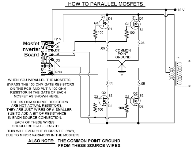
Fig-2: Parallel MOSFET Power Inverter


Circuit Credit: http://www3.telus.net/chemelec/Projects/Inverter/Mosfet-Inverter.htm

Wednesday, November 12, 2014

Booster for Input Impedance Circuit and explanation

The input impedance of a.c.-coupled op amp circuits depends almost entirely on the resistance that sets the d.c. operating point. If CMOS op amps are used, the input is high, in current op amps up to 10 MΩ. If a higher value is needed, a bootstrap may be used, which enables the input impedance to be boosted artificially to a very high value. In the diagram, resistors R1 plus R2 form the resistance that sets the d.c. operating point for opamp IC1. If no other actions were taken, the input impedance would be about 20 MΩ. However, part of the input signal is fed back in phase, so that the alternating current through R1 is smaller. The input impedance, Zin, is then: Zin=(R2+R3)/R3)(R1+R2). With component values as specified, Zin has a value of about 1GΩ. The circuit draws a current of about 3 mA.Circuit diagram:Input
Input Impedance Booster Circuit Diagram

Oxygen Sensor Simulator

This oxygen Sensor simulator is built from a 555 and few other common parts. Just when I thought Id seen all the uses for the 555. The oxygen sensor on a cars exhaust is used to determine how efficiently the fuel mixture is to an engine.

The oxygen sensor simulator as built on a protoboard. Note the cigarette lighter plug used for power source. The adjustment knob is at the left, and the switch is on the right. The red indicator LED is in the middle. Only use red, because the voltage drop of the LED is part of the circuit! 

A serial to parallel converter using the AT89C2051

A
The example program included with the PG2051 evaluation kit is a basic serial to parallel converter written in 8051 assembler. This is probably a good example of the uses to which an AT89C2051 can be put - it would be hard to get a serial to parallel converter much simpler than the single 20 pin IC in this circuit. The program is meant to serve as a useful example of 8051 serial routines and other programming, whether or not you actually need a serial to parallel converter.


Source: http://airborn.com.au/serial/sertopar.html

FM 9V transmitter circuit with expllanation

 9 volts circuit diagram transmitter
This circuit diagram transmitter is a very simple and useful circuit that require few external components and operates in FM band ( above 100 MHz ) . This circuit diagram transmitter needs to be powered from a 9 volts battery or from another 9 volts regulated power supply . The tuned coil L1, has two output tappings for the antenna connection, marked "A" and "B". These are both low-level outputs and you choose which tapping you want to use ( stable low range, or more unstable but higher range). Tap B (2.5%) takes just a very small portion of signal from the oscillator circuit and therefore gives a very frequency stable transmitter. The output level (around 2.5mW) and range are therefore somewhat reduced. Tap A (10%) delivers very much more power (around 10mW) to the antenna load. This gives you a greater range, but at the expense of frequency stability. All component leads should be kept as short as possible. The LINK wire on the PCB should lay flat on the PCB. Use the cutoff from a resistor leg. Antenna length for circuit diagram transmitter varies with frequency for optimum distance: 90MHz 80 cm, 95MHz 75cm, 100MHz 70 cm, 105 MHz 68 cm. The frequency determining elements (L1, C5 and C6) form a simple LC tuned oscillator. The inherent problem with this type of circuit diagram transmitter is that any external load (antenna) will change the operating frequency.

Tuesday, November 11, 2014

Photovoltaic Power System and Wiring Module Interconnection

Photovoltaic
Photovoltaic (PV) is the field of technology and research related to the application of solar cells for energy by converting sunlight directly into electricity. The following Photovoltaic Power System manual is a suggested practices manual examines the requirements of the 2005 National Electrical Code (NEC) as they apply to photovoltaic (PV) power systems. In this manual you will get the design requirements for the balance-of-systems components in a PV system are addressed, including conductor selection and sizing, overcurrent protection device rating and location, and disconnect rating and location.

This manual is divided into sections which covers discussion on Photovoltaic Modules (including Modules Marking, Wiring, Module Interconnection, Tracking Modules, Terminals, Transition Wiring, Module Connection Access, Module Connectors, and Splices), Conductor Color Code, PV Array Ground-Fault Protection, PV Array Installation and Service, Grounding (including size of DC grounding electrode conductor, point of connection, charge controller, ungrounded system), Equipment Grounding, Inverter AC Outputs, Conductor Ampacity, Overcurrent Protection, Batteries, Generators, Charge Controller, Inverters, Stand Alone Distribution System, etc.

Copper conductors are recommended for almost all photovoltaic system wiring. Copper conductors have lower voltage drops and better resistance to corrosion than other types of comparably sized conductor materials. Aluminum or copper-clad aluminum wires can be used in certain applications, but the use of such cables is not recommended—particularly in dwellings. All wire sizes presented in this guide refer to copper conductors.

Find more information about Photovoltaic Power System and Wiring Module Interconnection in the following manual. (source: scribd.com)

Sunday, November 9, 2014

Ampere or Current Booster

Small and very useful circuit, Can be built on a veroboard

Volt regulators such as the LM708, and LM317 series (and others) sometimes need to provide a little bit more current then they actually can handle. If that is the case, this little circuit can help out. A power transistor such as the 2N3772 or similar can be used.

The power transistor is used to boost the extra needed current above the maximum allowable current provided via the regulator.
Current up to 1500mA(1.5amp) will flow through the regulator, anything above that makes the regulator conduct and adding the extra needed current to the output load. It is no problem stacking power transistors for even more current. (see diagram). Both regulator and power transistor must be mounted on an adequate heatsink.

Circuit diagram:
Ampere or Current Booster Circuit Diagram

Parts:R1 = 1R-2W
R2 = 10R-2W
C1 = 35v-470uF
C2 = 35v-470uF
Q1 = TIP2955
IC1 = 78xx Regulator

Saturday, November 8, 2014

LM 3915 Sound Level Meter Circuit

This is a one chip sound level meter that can be use for displaying sound level of an amplifier or simply the sound level from a microphone.The heart of the circuit is IC LM 3915 Audio level IC.Even though it is a stand alone IC , a peak detector based on Transistor BC 558 and diode 1N4001 is also included for better performance.

Supply voltage can be from 3V to 20V.The input is set for audio line voltage (1V peak to peak) and has a max input voltage of 1.3V. To make the circuit use a moving dot display instead of bar graph display,Pin 9 can be should be disconnected from +V.

Part List

C1 2.2uF 25V Electrolytic Capacitor
C2, C3 0.1uF Ceramic Disc Capacitor
R1, R3 1K 1/4W Resistor
R2 10K 1/4W Resistor
R4 100K 1/4W Resistor
R5 1M 1/4W Resistor
D1 1N4001 Silicon Diode
Q1 BC 558 PNP Transistor
LED1-LED10 Standard LED or LED Array
U1 LM3915 Audio Level IC
MISC Board, Wire, Socket For U1

Simple Steam Whistle Circuit Diagram

This circuit consists of six square wave oscillators. Square waves are made up of a large number of harmonics. If six square waves with different frequencies are added together, the result will be a signal with a very large number of frequencies. When you listen to the result you’ll find that it is very similar to a steam whistle. The circuit should be useful in modelling or even in a sound studio.
Circuit diagram :

Simple Steam Whistle Circuit Diagram

This circuit uses only two ICs. The first IC, a 40106, contains six Schmitt triggers, which are all configured as oscillators. Different frequencies are generated by the use of different feedback resistors. The output signals from the Schmitt triggers are mixed via resistors. The resulting signal is amplified by IC2, an LM386. This IC can deliver about 1 W of audio power, which should be sufficient for most applications. If you leave out R13 and all components after P1, the output can then be connected to a more powerful amplifier. In this way a truly deafening steam whistle can be created. The ‘frequency’ of the signal can be adjusted with P2, and P1 controls the volume.

Simple Color Organ Circuit

Three Lamp-Channels Output Built-in Electret Microphone
A simple, satisfactory Color Organ can be built with a handful of cheap components. This design features: no mains supply transformer, built-in microphone and three widely adjustable frequency bands obtained by means of very simple, passive filters for Bass, Middle and Treble.
Circuit diagram :

Simple Color Organ Circuit Diagram
Due to the very low current consumption of this circuit, the mains supply can be conveniently reduced with no heat dissipation by the reactance of C1; then rectified by D1 and D2 and clamped to 24V by the Zener Diode D3. The music diffused by the loudspeaker(s) of any type of media player, is picked-up by the built-in microphone and the resulting signal is greatly amplified by a two-stage transistor audio amplifier Q1 and Q2.
At the output of the second stage, the audio signal is filtered and split into three fully adjustable frequency bands by means of a simple (though effective) passive filter formed by P1, P2, P3, R7, R8, C6 and C7, thus avoiding the complexity of op-amp based active filters. Transistors Q3, Q4 and Q5 are the drivers for the Triacs D4, D5 and D6 respectively, but can be omitted if high sensitivity Triac devices are used.
Parts:
P1,P2,P3_____10K   Linear Potentiometers
R1_____470R   1/2W Resistor
R2_____100K   1/4W Resistor
R3_____1M   1/4W Resistor
R4_____22K   1/4W Resistor
R5_____220K   1/4W Resistor
R6_____15K   1/4W Resistor
R7_____1K5  1/4W Resistor
R8_____4K7  1/4W Resistor
C1_____330nF  400V Polyester Capacitor
C2_____470µF   35V Electrolytic Capacitor
C3,C4,C6_____100nF   63V Polyester or Ceramic Capacitors
C5_____1µF   63V Electrolytic Capacitor
C7_____4n7   63V Polyester or Ceramic Capacitor
D1,D2_____1N4007 1000V 1A Diodes
D3_____BZX79C24   24V 500mW Zener Diode
D4,D5,D6_____TIC206M  600V 4A TRIACs
Q1 to Q5_____BC547   45V 100mA NPN Transistors
MIC1_____Miniature Electret Microphone Capsule
SW1_____SPST Toggle Switch 250V 10-15A (See Notes)
PL1_____Male Mains Plug
SK1,SK2,SK3_____Female Mains Sockets
Notes :
  • sing the Triac types suggested in the Parts List, each channel can drive several incandescent lamp bulbs, up to about 800W, but in this case a separate heatsink must be used for each Triac.
  • Due to the absence of a mains transformer, avoid to connect this circuit to other appliances (e.g. to the output of an amplifier by means of a cable). Please use only the microphone enclosed into the main case to pick-up the music.
  • For 110-120V mains operation, C1 value must be doubled: use two 330nF capacitors wired in parallel or one 680nF 250V capacitor. No further modification is required.
  • SW1 must be a high voltage, high current switch, as it must withstand the total amount of current drawn by all bulbs wired to the three outputs of the circuit.
Warning! The device is connected to 230Vac mains, then some parts in the circuit board are subjected to lethal potential! Avoid touching the circuit when plugged and enclose it in a plastic or wooden box.

Friday, November 7, 2014

Bass Booster Circuit

Increase the bass output of your present instrument at modest cost!
Bass Boost is todays sound... whether its the driving, gut-vibration pulsation of disco, or the solid bass line of soft, hard, or laid-back rock. One way to get the modern bass-boost sound without running out and buying an all-new expensive piece of equipment is to use a Bass Booster between your guitar, electronic organ or what-have-you, and the instrument amplifier. 

A bass booster strips the highs from the instruments output signal and amplifies low frequencies, feeding on "all-bass" sound to the instrument amplifier. Naturally, the bigger the speaker used with the amp, the more powerful the bass: use 15-inchers with the Bass Booster and you can rattle the windows. Bass Booster is powered by an ordinary 9 volt transistor radio battery. It can be assembled on a small printed board or on a veroboard using point to point wiring. The booster connects between your instrument and its amplifier through two standard RCA Jacks.

Circuit Diagram:
 Bass Booster Circuit Diagram
Parts:
P1 = 50K
P2 = 100K
R1 = 22K
R2 = 470K
R3 = 47K
R4 = 10K
R5 = 470R
R6 = 1K
Q1 = 2N2222
C1 = 2.2uF-25v
C2 = 100nF-63v
C31 = 00nF-63V
C4 = 3.3uF-25v
C5 = 470uF-25v
D1 = 5mm. Red Led
Q1 = 2N2222
B1 = 9v Battery
J1 = RCA Audio Input Socket
J2 = RCA Audio Output Socket
S1 = On-Off SwitchUsing Bass Booster:
Connect your electronic guitar or other electronic instrument to input jack J1; Connect output jack J2 to your instruments amplifiers normally-used input. With power switch S1 off, key S2 so the instrument feeds directly to the instrument amplifier. With P2 set full counter-clockwise (Off), turn power switch S1 on, key S2 once, and advance P2 for the desired Bass Boost level. To cut back to natural sound just stomp down on S2 and key the Bass Booster out. Dont worry about leaving power switch S1 on for several hours of a gig. The circuit pulls less than 1mA from the battery, so battery will last many, many months.

Little Door Guard

If some intruder tries to open the door of your house, this circuit sounds an alarm to alert you against the attempted intrusion. The circuit (Fig. 1) uses readily available, low-cost components. For compactness, an alkaline 12V battery is used for powering the unit. Input DC supply is further regulated to a steady DC voltage of 5V by 3-pin regulator IC 7805 (IC2).


Fig. 1: Circuit of the door guard

Assemble the unit on a general-purpose PCB as shown in Fig. 4 and mount the same on the door as shown in Fig. 3. Now mount a piece of mirror on the door frame such that it is exactly aligned with the unit. Pin configurations of IC UM3561 and transistors 2N5777 and BC547 are shown in Fig. 2. 


Fig. 2: Pin configurations of UM3561 and transistors 2N5777 and BC547

Initially, when the door is closed, the infrared (IR) beam transmitted by IR LED1 is reflected (by the mirror) back to phototransistor 2N5777 (T1). The IR beam falling on phototransistor T1 reverse biases npn transistor T2 and IC1 does not get positive supply at its pin 5. As a result, no tone is produced at its output pin 3 and the loudspeaker remains silent. Resistor R1 limits the operating current for the IR LED.
When the door isopened, the absence of IR rays at phototransistor T1 forward biases npn transistor T2, which provides supply to  positiveIC1. Now 3-sirensound generator IC UM3561 (IC1) gets power via resistor R5. The output of IC1 at pin 3 is amplified by Darlington-pair transistors T3 and T4 to produce the alert tone via the loudspeaker. 


Fig. 3: Back view of the door assembly

Rotary switch S2 is used to select the three preprogrammed tones of IC1. IC1 produces fire engine, police and ambulance siren sounds when its pin 6 is connected to point F, P or A, respectively.
Fig. 4: Suggested enclosure with major components layout

Thursday, November 6, 2014

Morning Alarm Circuit Diagram based LDR

This LDR based alarm can be used as get up alarm. The Alarm turns on in the morning automatically and turns off only when manually switched off ,so you will have to get up. It is a simple LDR based light sensor circuit.

LDR or Light Dependent Resistor is a kind of variable resistor and its resistance depends on the intensity of light falling on it. In complete dark, its resistance is as high as 1 Meg Ohm, but it reduces to 100 ohms or less in full light. So it is an ideal device to use as light switch. Sensitivity of LDR depends on its size also. Commonly available sizes are 3mm, 5mm, 10mm etc. But costly types with greater sensitivity are also available.

When the circuit is place in dark, near the window, LDR fails to conduct and T1 will not get base bias. So it remains off and buzzer will be silent. When the sunlight falls on LDR, IN the morning, LDR conducts and provides base bias to T1. T1 then conducts to activate the buzzer. Capacitor C1 is provided for the clean switching of T1. T1 will conduct only when C1 is charged fully. This prevents chirping sound during light transition.You can use an easily available Music buzzer to get melody tone.

9V Automatic Battery NiCd Charger

This automatic NiCd charger for 9V NiCd batteries is using 555 timer properties and is very easy to build. Why is an automatic 9 volts NiCd battery charger? Because you can leave the battery for charging as much as you like: it will be always completely charged and ready for use when is needed. It wont be overcharged and it will not discharge.

9V Automatic Battery NiCd Charger Circuit Diagram :

charger-circuit-diagram

With the values presented in the circuit diagram, the battery charger NiCd circuit is suitable for 6V and 9V batteries. 9 volt types with 6 and 7 cells are charging with 20mA; P1 must be adjusted so that the NiCd charger disconnects after 14 hours. Window inferior level is set at 1V below this value with P2. 5V battery type with 4 or 5 cells are charged at 55mA. Again, with P1 adjust the NiCd charger circuit so it disconnects after 14 hours. Window inferior level must be set at 0.8V below this value.


Video Tracer Circuit Diagram

This circuit was designed as an aid to installers and maintainers of video systems. It is basically a video sync separator (IC1) followed by a LED and buzzer driver (IC2, Q1 & Q2). In use, the device is connected to a video cable and if there is video present, the LED will flash at about 10Hz. If there is no video, the LED flashes briefly every couple of seconds. A buzzer can also be switched in to provide an audible indication. The buzzer is particularly useful when tracing cabling faults or trying to find a correct cable amongst many, where it is difficult to keep an eye on the LED.

Another use for the buzzer option is to provide a video fault indication. For example, it could be inserted in bridging mode, with switch S1 in high impedance mode (position 2) across a video line and set to alarm when there is no video present. If someone pulls out a cable or the video source is powered off, the alarm would sound. IC1 is a standard LM1881 video sync separator circuit and 75Ω termination can be switched in or out with switch S1a. The other pole of the switch, S1b, turns on the power. The composite sync output at pin 1 is low with no video input and it pulses high when composite sync is detected.

Video Tracer Circuit diagram:

video

These pulses charge a 100nF capacitor via diode D1. When there is no video at the input, oscillator IC2b is enabled and provides a short pulse every couple of seconds to flash the LED. The duty cycle is altered by including D2, so that the discharge time for the 10μF capacitor is much shorter than the charge time. The short LED pulse is used as a power-on indicator drawing minimal average current. When video is present at the input, IC2b is disabled and IC2d is enabled. The output of IC2d provides a 10Hz square wave signal to flash the LED. The buzzer is controlled by switch S2. In position 2 the buzzer will sound when there is video at the input and in position 1 the buzzer will sound when there is no video at the input.


Wednesday, November 5, 2014

Laser Level Detector

Rotating laser levels, which are very handy  for setting objects in a room or garden at the  same height, are available at prices of a few  dozen pounds. At relatively large distances  and for outdoor use, the light from the rotating laser beam is often not easy to see, and  the laser beam detector described here can  be useful in such situations. The detector  works well at distances up to 50 metres (150  feet) and consists entirely of standard components. The detector is housed in a plastic case  that can be fixed to an object (such as a post  or a beam). It has three LEDs and a beeper that  indicate whether the object should be raised  or lowered. 
Laser
LEDs with a transparent package and integrated lens (round surface) are used as sensors. The top and bottom detection zones  each have five LEDs and two opamps (IC1a &  IC1b or IC1c & IC1d), which drive the ‘Move  Up’ and ‘Move Down’ indicator LEDs. The middle sensor LED drives the ‘OK’ indicator LED  via two opamps (IC2a & IC2b).  The rising edges of the opamp output signals  trigger three separate monostable multivibrators (type CD4047). If desired, the circuit  shown inside the dashed outline (one gate of a  CD4044 quad RS latch) can be used in place of  each of the monostable multivibrators. In this  case the output signal has the opposite polar-ity, so the BS170 N-channel MOSFET must be  replaced by a P-channel type. 
Laser

The monostable time of the middle retriggerable MMV should be longer than the rotation period of the laser (e.g. with a 2 rpm laser  it should be longer than 500 ms) so that the  beeper will emit a continuous tone. Most  rotating laser levels have variable speed, so  this can also be achieved by adjusting the peed if necessary. The monostable times of  the upper and lower MMVs are dimensioned  to generate clearly distinguishable short and  long beeps, respectively. The three MOSFETs  (T1, T2 and T3) are configured as a wired-OR  gate to drive the shared beeper. The fourth  MOSFET (T4) drives the ‘OK’ LED. 
The circuit can be housed in an enclosure  together with three penlight cells.


Spy Camera Solar Power Box

Battery life has always been a critical consideration for most of the electronic gadgets and equipment. When we talk about spy  cameras,  which  normally  function  round-the-clock, they often run out of power within a few days.  Many spy cameras (CCTV cameras) are powered by 9V PP3 type batteries that offer five times more energy  than the regular 9V alkaline battery.

Mini CCTV cameras also accept 6-12V DC supply from AC mains adaptor through the DC IN jack. AC mains adaptor for the camera increases the capacity of the 9V PP3 battery but is bulky and noisy. Whether disposable  or rechargeable batteries, making frequent replacement or recharging them is a cumbersome job. The unique solar power box described here serves an alternative solution to the problem. 

Spy Camera Solar Power Box Circuit diagram :

Spy

The circuit of the solar power box is simple. It contains a  battery charger and a battery health indicator and  a few other components.  As shown in the circuit,  DC supply available from  the solar panel (SP1) is  directly applied to the in-put of the circuit through  a protection diode (D1).  This diode is used to pre-vent  the  reverse  current  flow from the battery to  the  solar  panel  during  night. Thus, D1 allows  the current to flow from the solar panel  to the battery only. Low-voltage-drop  type 1N5817 diode is perfect for the  job.
At the heart of the circuit is an integrated current source, realised using a  popular 3-pin adjustable voltage regulator LM317T(IC1). 

This IC is designed  to adjust its internal resistance between  the In (pin 3) and Out (pin 2) terminals  to maintain a constant voltage of 1.25V  between the Out (pin 2) and Adj (pin 1) terminals. Here, a 9V, 280 mAh  rechargeable PP3 type Ni-MH battery  (BATT) is used as reservoir. Normally,  a charging current of about 10 per cent  of  ampere-hour  rating  is  safe  for  the  battery. Resistor R1 (39-ohm, 0.5W),  connected between pin 1 and 3 of IC1,  limits  the  charging  current  to  about  30 mA. DC output from the battery is  available at output jack J2. Red LED  ( LED1) is used as a battery ‘health’  indicator. Switch S1 is used to start the  charging while S2 is used for connect-ing the load. Note that suitable heat  sink should be used for the IC1.

The proper selection of solar panel  is important but not critical. A miniature 12V type solar panel with a cur-rent output of about 100 mA can be  used. Even if you have a solar panel  with  higher  voltage  rating,  it  will  not  create a problem as the circuit ensures  that the charging current cannot exceed  the predetermined value.

The circuit can be easily assembled  on a general-purpose PCB and housed  in a small plastic cabinet.


500W Low Cost 12V to 220V Inverter

Using this circuit you can convert the 12V dc in to the 220V Ac. In this circuit 4047 is use to generate the square wave of 50hz and amplify the current and then amplify the voltage by using the step transformer. How to calculate transformer rating
inverter

The basic formula is P=VI and between input output of the transformer we have Power input = Power output
For example if we want a 220W output at 220V then we need 1A at the output. Then at the input we must have at least 18.3V at 12V because: 12V*18.3 = 220v*1
So you have to wind the step up transformer 12v to 220v but input winding must be capable to bear 20A.

Note :This Circuit is using high voltage that is lethal. Please take appropriate precautions


Tuesday, November 4, 2014

Simple Smoggy

Even if your good old (Sony) Walkman  sees little use nowadays it would be a  shame to get rid of it altogether. The more  so when just removing the tape head  would allow the built-in audio amplifier  to become an outstanding electrosmog  detector for a variety of purposes. Looking at the schematic, readers with RF  experience will have no difficulty in recognising the diodes and coils of the two  detector-receivers, which serve to capture and demodulate RF signals. With its  coil of four turns (L2) one receiver covers the higher frequency range of the  electromagnetic waves, whilst the sec-ond detector takes care of the lower frequency range.

Simple Smoggy Circuit diagram:

Simple

For this reason a coil with a  greater number of turns is required: L1 is  an RF choke of about 250 µH. The precise  value is not critical and it could equally be  220 µH or 330 µH. The outputs of both detector-receivers  are connected to the cables disconnected  previously from the tape heads, feeding the  right and left channel inputs to the Walk-man’s audio amplifier. Please note here that  the screening of the tape head cable does not  have to be absolutely identical to the ground connection of the amplifier circuitry. As  we are dealing with a stereo amplifier,  we are listening into both channels and  thus both RF ranges at the same time.

One channel of the amplifier can also be  used to demodulate low-frequency magnetic alternating fields  via a capacitor  (C3) bypassing diode D1 and connecting either a third coil (L3, for instance;  a telephone recording adapter) as the  pickup device or else a long piece of wire  for acquiring low frequency AC electrical fields. Sources like this are discernible mainly by a distinct 50 Hz (or 60 Hz)  humming in the earphones. Predicting what you may hear down to  the very last detail is difficult, since every  locality has its own, individual interference sources. Nevertheless, with practice  users will succeed in identifying these  interference sources by their particular  audio characteristics.

To sum up, four different ‘sensors’ can be  connected to the inputs of this circuit:  ANT1 (approx. 50 cm long whip antenna),  ANT2 (3.5 cm short stub antenna), ANT3  (approx. 1 m long wire antenna for low frequency electrical fields) and a coil for magnetic fields. Finally, two more tips:
  1. Use only ‘good old’ germanium diodes for  D1 and D2. Sensitivity will be much reduced if  silicon diodes are used, as these have a higher  threshold voltage.
  2. Smoggy does not provide an absolute indi-cation of field strength and even more so can-not provide any guidance whether anything  it detects might be harmful. Its function is to detect electromagnetic signals and compare  their relative magnitude.

    Author : Tony Ruepp  - Copyright : Elektor


    10 Watt Car Audio Amplifier

    10 Watt Car Audio AmplifierTDA2003 is audio amplifier integrated circuit chip in 10 Watt class. All you need is just adding few passive components and your amplifier will be ready. You can even amplify ultrasonic range if you wish to abuse its usage, just to convince you that this chip is more than enough to handle any range of audio signal. Although many manufacturer produce this TDA2003 chip, in general, this various chip from various manufacturer normally comply with these following features: Short circuit protection between all pins, High current output ( up to 3 A), Built-in Over temperature protection, and Low harmonic and crossover distortion.
    https://blogger.googleusercontent.com/img/b/R29vZ2xl/AVvXsEgygMdSQK-z3b-3rinGaMuNjrG2BqwyLe5RD0hy3-Ljbtk59WTPdcjYE_ZjOmGkFzbXSQYoO17BpE9onPp-aF8yyusNMlfox-2W7Dernar1FfcCEspWn_-PzxRi8uh57EU2uBWRJLXhhYO7/s1600/Amplifier+stereo+with+turbo+bass.jpg

    Voltage Controlled Oscillator

    In most cases, the frequency of an oscillator is determined by the time constant RC. However, in cases or applications such as FM, tone generators, and frequency-shift keying (FSK), the frequency is to be controlled by means of an input voltage, called the control voltage. This can be achieved in a voltage-controlled oscillator (VCO). A VCO is a circuit that provides an oscillating output signal (typically of square-wave or triangular waveform) whose frequency can be adjusted over a range by a dc voltage.

    Voltage Controlled Oscillator Block Diagram :

    Voltage

    An example of a VCO is the 566 IC unit, that provides simultaneously the square-wave and triangular-wave outputs as a function of input voltage. The frequency of oscillation is set by an external resistor R1 and a capacitor C1 and the voltage Vc applied to the control terminals. Figure shows that the 566 IC unit contains current sources to charge and discharge an external capacitor Cv at a rate set by an external resistor R1 and the modulating dc input voltage.

    A Schmitt trigger circuit is employed to switch the current sources between charging and discharging the capacitor, and the triangular voltage produced across the capacitor and square-wave from the Schmitt trigger are provided as outputs through buffer amplifiers. Both the output waveforms are buffered so that the output impedance of each is 50 f2. The typical magnitude of the triangular wave and the square wave are 2.4 Vpeak.to-peak and 5.4Vpeak.to.peak.

    The frequency of the output waveforms is approximated by : fout = 2(V+ - Vc)/R1C1V+

    Voltage Controlled Oscillator Circuit Diagram :

    VCO-Circuit-Diagramw

    Figure shows the pin connection of the 566 unit. The VCO can be programmed over a 10-to-l frequency range by proper selection of an external resistor and capacitor, and then modulated over a 10-to-l frequency range by a control voltage, Vc The voltage controlled oscillators (VCOs) are commonly used in converting low-frequency signals such as EEG (electro-encephalograms) or ECG (electro-cardiograms) into an audio­frequency (AF range).


    Monday, November 3, 2014

    Low Cost Playback Amplifier For Cassette Deck

    For some time now, there have been a number of tape cassette decks available at low prices from mail order businesses and electronics retailers. Such decks do not contain any electronics, of course. It is not easy to build a recording amplifier and the fairly complex magnetic biasing circuits, but a playback amplifier is not too difficult as the present one shows.

     The stereo circuits in the diagram, in conjunction with a suitable deck, form a good-quality cassette player. The distortion and frequency range (up to 23 kHz) are up to good standards. Moreover, the circuit can be built on a small board for incorporation with the deck in a suitable enclosure. Both terminals of coupling capacitor C1 are at ground potential when the amplifier is switched on.

     Cassette Deck Playback Amplifier Circuit Diagram:


    Because of the symmetrical ±12 V supply lines, the capacitor will not be charged. If a single supply is used, the initial surge when the capacitor is being charged causes a loud click in the loudspeaker and, worse, magnetizes the tape. The playback head provides an audio signal at a level of 200–500 mV. The two amplifiers raise this to line level, not linearly, but in accordance with the RIAA equalization characteristic for tape recorders. Broadly speaking, this characteristic divides the frequency range into three bands:
    • Up to 50 Hz, corresponding to a time constant of 3.18 ms, the signal is highly and linearly amplified.
    • Between 50 Hz and 1.326 kHz, corresponding to a time constant of 120 µs, for normal tape, or 2.274 kHz, corresponding to a time constant of 70 µs, for chromium dioxide tape, the signal is amplified at a steadily decreasing rate.
    • Above 1.326 kHz or 2.274 kHz, as the case may be, the signal is slightly and linearly amplified. This characteristic is determined entirely by A1 (A1’). To make the amplifier suitable for use with chromium dioxide tape, add a double-pole switch (for stereo) to connect a 2.2 kΩ resistor in parallel with R3 (R3’). The output of A1 (A1’) is applied to a passive high-pass rumble filter, C3-R5 (C3’-R5’) with a very low cut-off frequency of 7 Hz. The components of this filter have exactly the same value as the input filter, C1-R1 (C1’-R1’). The second stage, A2 (A2’) amplifies the signal ´100, that is, to line level (1V r.m.s.).

    Car Stereo Booster with LM2896

    Car Stereo Booster with LM2896This car stereo booster uses an LM2896 IC which has two integrated amplifiers. It can be powered with voltages up to 15 volts. The power output is 2.5 watts per channel with an 8 Ω load and supply voltage of 12 volts. Using the bridge tehnique in the circuit gives a power output of 9 watts. The car audio booster can be powered up from 3 up to 15 volts.
    Car stereo booster circuit diagram
    https://blogger.googleusercontent.com/img/b/R29vZ2xl/AVvXsEgUNr6P5hgSNMIKiTq5zeSaQrj_Rvl39JbQ1NgipvZ4wBpRbUDinwjNbAmjA5XE0javjrLGd8EE6YQVlhlOCk4MLoAbpA2vZA2Iw_GR7PM9FFhcjyGVgKmO5oUEfO-VnTDhOOFRH9ZKrGf_/s400/20W+Car+Audio+Amplifier+with+LM1875.png
    The load impedance that can be connected at its output can be either 4 Ω or 8 Ω. The supply voltage and the load impedance influence the output power level. This amplifier circuit is designed as a booster for auto radio/cassette players. The current consumption by maximum power output and a 4 Ω load is 1 ampere.