Showing posts with label a. Show all posts

Monday, November 17, 2014

Make A Virtual Phone Battery

Virtual cell phone battery is a replacement cell phone batteries for those of you who use the phone as a modem. Including myself, who use the phone as a modem HAIER d1200p internet.  Why must use this virtual battery. For those who surf hobby "full time" with a phone modem, would know the problem, the battery gets hot and fast reply wasteful even worn out.
virtual
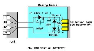
This tool is a good solution to keep and care for our cell phones from the possibility of damage from over-charging its battery.I created a virtual battery works as follows:We take the source of its power supply from the USB port because the port is very easy and simple to use and simply provide a standard current source when the phone is online (500-750mA).

The workings of the circuit is as follows:Diodes or diode 2Amper in 5239 this standard to provide a useful addition to the polarity of the voltage which is also a component of protection against misuse. You can just use a 1 Amp diode (IN4002-4007). I use the IN 5239 is due to be durable, more resistant to heat.4v3 zener diode IN4007 and configured to create a portal voltage of 5V (4.3 + 0.7 volt zener Vin4007) and is useful as a protection system against possible voltage spikes in the event of damage to the CPU.220nF capacitor as a stabilizer and a substitute for the original battery cells.

The following also 100pF capacitor to smooth and filter the dc current through the diode 5239 which came out of the induction logging.Configuration between zener4v3, IN4007 diode and C 220n form a cell replacement from the actual battery cells, because the battery was actually a capacitor which had a large capacity.You can just remove the three components mentioned above. although it can work fine .

But results are not as good as that use virtual cell (replacement), which certainly was the security which we have to think to avoid the things which are not in want.Making way is to use an old cell phone batteries which have been wasting his cell, a raft of this circuit and the solder terminals on the batteries with the polarity distinguished. Make two holes for the cable to the jack / USB jack.

 Determine the length of cable required to taste and use stranded cable with a diameter of at least 1mm.If some type of cell phone batteries are very thin, use a small box for this circuit and connect the two wires to the output voltage again for hp battery casing. Or also if you do not have a former battery casing, use alligator clips to the battery terminal on the phone .. Pin the middle of the virtual pin replacement battery is BSI (Battery Size Insdicator) is useful for HP Nokia.

Class A MOSFET Amplifier 2SK1058


This is simple class A MOSFET amplifier 2SK1058 used in the circuit. It is easy to do, you should use a 24V supply volt at high current. using amplifier with Class A tube preamp based on 12AU7. It produces the purest sound. I have no idea of ​​the levels of distortion, but has a very fine and delicate texture quality. With only one watt speaker output should be used efficiently. Lower is better than expected and the stage design of the units of my 12 "base 63L 3-way speakers with ease.

Wednesday, November 12, 2014

A serial to parallel converter using the AT89C2051

A
The example program included with the PG2051 evaluation kit is a basic serial to parallel converter written in 8051 assembler. This is probably a good example of the uses to which an AT89C2051 can be put - it would be hard to get a serial to parallel converter much simpler than the single 20 pin IC in this circuit. The program is meant to serve as a useful example of 8051 serial routines and other programming, whether or not you actually need a serial to parallel converter.


Source: http://airborn.com.au/serial/sertopar.html

Saturday, September 20, 2014

25W Class A Power Audio Amplifier Wiring diagram Schematic

This is the 25W Class-A power audio amplifier schema. The output devices are MJL4281A (NPN) and MJL4302A (PNP), and have high bandwidth, fantastic SOA (safe operating area), high linearity and high gain. Driver transistors are MJE15034 (NPN) and MJE15035 (PNP). All devices are rated at 350V, using the power transistors having a 230W dissipation and the drivers are 50W.

25W Class-A Power Audio Amplifier Circuit Diagram

Build


  •  The supply voltage must be a maximum of ±25V. This supply is simply obtained from a 20-0-20V transformer, recommended current is 1A.
  •  All resistors ought to be 1/4W or 1/2W 1% metal film for lowest noise, with the exception of R9, R10 and R15 which ought to be 1/2W varieties, and R13, R14 have to be 5W wirewound.
  •  Using the suggested and advised 25V supplies, Q4 will typically not need a heatsink. The output drivers (Q5 and Q6) recommended to use a heatsink, even though it doesn’t have to be big.

Friday, September 12, 2014

10 to 14W Class A Audio Amplifier Wiring diagram Schematic

I have built this amplifier and it does sound good. It requires a preamp as it hasnt got much gain. It requires big heat sinks and a large transformer and a great power supply and careful wiring, but in the end it is xtremely simple and it sounds very good. The zener diode rejects any ripple coming from the power supply, But you still only want a ripple of 10mV max. The ripple reaching the input is amplified, so the zener diode gets rid of that, but whatever ripple there is will still reach the power stage.

10

Thursday, September 11, 2014

Hi Fi 25W Power Amplifier Class A

Hi-Fi 25W Power Amplifier (Class-A) Schematics Circuit
Hi-Fi
Click to view larger

Friday, September 5, 2014

Build a Relay Switch Activated by Tone and Signal

The essence of the schema is for the input of tone and signal to provide an activation for the relay switch.
  • Relay – an electrically operated switch where the current flowing through the coil of the relay is creating a magnetic field which attracts a lever and changes the switch contacts, thereby making its state open or close
  • BC214 – a complementary silicon planar epitaxial transistor used in AF small signal drivers and am1 as well as for low noise preamplifier applications due to its feature of good linearity of DC current gain
  • LM741 – a general purpose single operational amplifier with features such as offset null, compensated internal freq uency, voltage range with high input, good stability of temperature, and protected from short schema
The use of relay will allow the schema to switch from one condition to another. It can also be referred to as a form of an electrical amplifier since it is able to control an output schema of higher power than the input schema. There are many types of relays being used in many electronic and electrical diagram, which include solid-state relay, Buchholz relay, overload protection relay, latching relay, forced-guided contacts relay, mercury-wetted relay, contactor relay, machine tool relay, reed relay, polarized relay, and solid state contactor relay.

 Relay Switch Activated by Tone and Signal Circuit Diagram

Build
The schema created is sensitive enough to the AC signals in the input stage, where the signals are ranging above 5 mV. It will also be sensitive to react with the human voice signals having a range of frequency from 50 Hz up to 3 KHz. The human voice is a part of the human sound produced primarily by the vocal cords or vocal folds which in turn produces a voice frequency that is used for the transmission of speech.

During the absence of an input signal, the state of the 12 V relay RL1 is at OFF condition as regulated by the 10K Ohms trimmer RV1. The schema can be made to react with its sensitivity in points A, B, & C, where a negative feedback can be placed due to the addition of band pass filter. The filter will operate only in the 1 KHz range and the schema will only correspond at this frequency.
Relay

The signal and tone activated relay switch were used in a wide range of fields which includes measuring instruments, audio systems, communications equipment, and factory-automation equipment. They can also be found on telephone subscriber diagram for the polarity reversing switch, testing, and ringing functions.

Thursday, September 4, 2014

How to fix a tube light simply


This post shows how to fix a tube light with its parts correctly.lots of people asked me about this that is why I thought to give you some thing like this.now I think you will be able to solve your problems.


Note

# Be careful when you deal with 230v current.

#kids should not test this schema.

Tuesday, September 2, 2014

Use the CD ROM drive as a audio CD player without the computer


Most of the CDROMS available have an Audio-Out Output to either plug in the headphones or connect it to an amplifier.This schema enables one to use the CDROM as a stand alone Audio CD player without the computer.This schema is nothing but a power supply which supplies +5v, +12V and Ground to the CDROM drive and
hence can be used without the computer.


http://www.electronic-diagram-diagrams.com/audioimages/4.gif
You should buy a D-type power connecter to connect this diagram outputs to the CDROM. The details of the D connector are shown along with the schema diagram. Note that the D-connector goes into the CDROM in only one way and hence prevents any damage due to wrong connection. Ensure that the 12V(yellow) wire is connected to the right of the D-connector(as seen from behind ,i.e the connector holes away from you with the curved portion of the connector upwards) As soon as an Audio CD is inserted, the CD begins to play. To move to the next track, press the Skip-Track button on the CDROM front Panel.

Monday, September 1, 2014

Build a Car Voltage Regulator Circuit Using LM317

The car cigarette lighter socket does not only light cigarettes, but can be utilized as an electrical channel for powering tools to work on the car such as laptops and other electronic devices. The following schema diagram shows a way of powering a two-way mobile radio using the LM317T voltage regulator.

The LM317T is an adjustable 3-terminal positive voltage regulator that efficiently provides a load current of 1.5 Amps over an output range of 1.2 V and 37 V. With reference to the schema, it can accept 14 volts without any hassle and the voltage can be controlled easily with the use of a potentiometer, a 3-terminal resister with sliding contact. The whole schema will contain the following components:


 Printed Circuit Board (PCB)
Resistor 1 (R1): 270 ohms
Resistor 2 (R2): 2K carbon potentiometer
Capacitor 1 (C1): 100nF
Capacitor 2 (C2): 1uF tantalum
LM317T Voltage Regulator
Heat Sink
DC Power Jacks
Green LED: Power
Red LED: Over Voltage
Zener Diode: over voltage LED switch

The zener diode switches on the over voltage LED if the voltage passing through is larger than the breakdown or preset voltage. The use of zener diode permits a constant amount of voltage and can be very beneficial for devices that inputs the same amount of voltage.

LM317T is cheaply available in the market and is very simple to integrate into several energy system to supply a maximum current or voltage.

Sunday, August 31, 2014

A Low Cost Hearing Aid Circuit

Small and portable unit, Useful for old men and old women

This low-cost, general-purpose electronic hearing aid works off 3V DC (2x1.5V battery). The schema can be easily assembled on a veroboard. For easy assembling and maintenance, use an 8-pin DIP IC socket for TDA2822M.

Circuit Diagrams:
Hearing A Low Cost hearing Aid Circuit
Parts:
P1 = 10K
R1 = 2.2K
R2 = 330K
R3 = 680R
R4 = 33R
R5 = 100R
R6 = 4.7R
R7 = 4.7R
R8 = 220R
C1 = 0.01uF-10V
C2 = 100nF-63V
C3 = 47uF-10V
C4 = 10uF-10V
C5 = 0.01uF-10V
C6 = 100uF-10V
C7 = 100nF-63V
C8 = 100nF-63V
D1 = Red LED
Q1 = BC547
IC1 = TDA2822M
EP1 = Mono Earphone 32R
SW1 = On-Off Switch

Circuit Operation:

In this schema, transistor Q1 and associated components form the audio signal preamplifier for the acoustic signals picked up by the condenser microphone and converted into corresponding electrical signals. Resistor R5 and capacitor C3 decouple the power supply of the preamplifier stage. Resistor R1 biases the internal schema of the low-voltage condenser microphone for proper working. The audio output from the preamplifier stage is fed to the input of the medium-power amplifier schema via capacitor C2 and volume control P1.

The medium-power amplifier section is wired around popular audio amplifier IC TDA2822M (not TDA2822). This IC, specially designed for portable low-power applications, is readily available in 8-pin mini DIP package. Here the IC is wired in bridge configuration to drive the 32-ohm general-purpose monophonic earphone. Red LED (D1) indicates the power status. Resistor R8 limits the operating current of D1. The audio output of this schema is 10 to 15mW and the quiescent current drain is below 1 mA.

Source : electronsforu

How to Build a Photodiode current to voltage converter

The Photodiode current-to-voltage converter schema uses three CA3130 BiMOS op amps in an application sensitive to sub-picoampere input currents. The schema provides a ground-referenced output voltage proportional to input current flowing through the photo-diode.

 Photodiode current-to-voltage converter schema


Save Your Ears A Noise Meter

‘Hello… HELLO! Are you deaf? Do you have disco ears?’ If people ask you this and you’re still well below 80 , you may be suffering from hearing loss, which can come from (prolonged) listening to very loud music. You won’t notice how bad it is until it’s too late, and after that you won’t be able to hear your favorite music the way it really is – so an expensive sound system is no longer a sound investment. To avoid all this, use the i-trixx sound meter to save your ears (and your neighbors ears!).
With just a handful of components, you can build a simple but effective sound level meter for your sound system. This sort of schema is also called a VU meter. The abbreviation ‘VU’ stands for ‘volume unit’, which is used to express the average value of a music signal over a short time. The VU meter described here is what is called a ‘passive’ type. This means it does not need a separate power supply, since the power is provided by the input signal. This makes it easy to use: just connect it to the loudspeaker terminals (the polarity doesn’t matter) and you’re all set.
The more LEDs that light up while the music is playing, the more you should be asking yourself how well you are treating your ears (and your neighbours’ ears). Of course, this isn’t an accurately calibrated meter. The schema design is too simple (and too inexpensive) for that. However, you can have a non-disco type (or your neighbors) tell you when the music is really too loud, and the maximum number of LED lit up at that time can serve you as a good reference for the maximum tolerable sound level.
Although this is a passive VU meter, it contains active components in the form of two transistors and six FETs. Seven LEDs light up in steps to show how much power is being pumped into the loudspeaker. The steps correspond to the power levels shown in the schematic for a sine-wave signal into an 8-ohm load. LED D1 lights up fi rst at low loudspeaker voltages. As the music power increases, the following LEDs (D2, D3, and so on) light up as well. The LEDs thus dance to the rhythm of the music (especially the bass notes).
Circuit diagram:
noise Noise Meter Circuit Diagram
This schema can easily be assembled on a small piece of prototyping board. Use low-current types for the LEDs. They have a low forward voltage and are fairly bright at current levels as low as 1 mA. Connect the VU meter to the loudspeaker you want to monitor. If LED D2 never lights up (it remains dark even when LED D3 lights up), reverse the polarity of diode D8 (we have more to say about this later on). In addition, bear in mind that the sound from the speaker will have to be fairly loud before the LEDs will start lighting up.
If you want to know more about the technical details this VU meter, keep on reading. Each LED is driven by its own current source so it will not be overloaded with too much current when the input voltage increases. The current sources also ensure that the final amplifier is not loaded any more than necessary. The current sources for LEDs D1–D6 are formed by FET diagram. A FET can be made to supply a fixed current by simply connecting a resistor to the source lead (resistors R1–R6 in this case). With a resistance of 1 kΩ, the current is theoretically limited to 1 mA. However, in practice FETs have a especially broad tolerance range. The actual current level with our prototype ranged from 0.65 mA to 0.98 mA.
To ensure that each LED only lights up starting at a defined voltage, a Zener diode (D8–D13) is connected in series with each LED starting with D2. The Zener voltage must be approximately 3 V less than the voltage necessary for the indicated power level. The 3-V offset is a consequence of the voltage losses resulting from the LED, the FET, the rectifier, and the over voltage protection. The over voltage protection is combined with the current source for LED D7. One problem with using FETs as current sources is that the maximum rated drain–source voltage of the types used here is only 30 V.
If you want to use the schema with an especially powerful fi nal amplifier, a maximum input level of slightly more than 30 V is much too low. We thus decided to double the limit. This job is handled by T7 and T8. If the amplitude of the applied signal is less than 30 V, T8 buffers the rectified voltage on C1. This means that when only the first LED is lit, the additional voltage drop of the over voltage protection schema is primarily determined by the base–emitter voltage of T8. The maximum worst-case voltage drop across R8 is 0.7 V when all the LEDs are on, but it has increasingly less effect as the input voltage rises.
R8 is necessary so the base voltage can be regulated. R7 is fitted in series with LED D7 and Zener diode D13, and the voltage drop across R7 is used to cause transistor T7 to conduct. This voltage may be around 0.3 V at very low current levels, but with a current of a few mili-amperes it can be assumed to be 0.6 V. Transistor T7 starts conducting if the input voltage rises above the threshold voltage of D7 and D13, and this reduces the voltage on the base of T8. This negative feedback stabilizes the supply voltage for the LEDs at a level of around 30 V. With a value of 390 Ω for R7, the current through LED D7 will be slightly more than 1 mA.
This has been done intentionally so D7 will be a bit brighter than the other LEDs when the signal level is above 30 V. When the voltage is higher than 30 V, the schema draws additional current due to the voltage drop across R8. The AC voltage on the loudspeaker terminals is half-wave rectifi ed by diode D14. This standard diode can handle 1 A at 400 V. The peak current level can be considerably higher, but don’t forget that the current still has to be provided by the fi nal amplifier.
Resistor R9 is included in series with the input to keep the additional load on the fi nal amplifi er within safe bounds and limit the interference or distortion that may result from this load. The peak current can never exceed 1.5 A (the charging current of C1), even when the schema is connected directly to an AC voltage with an amplitude of 60 V. C1 also determines how long the LEDs stay lit. This brings us to an important aspect of the schema, which you may wish to experiment with in combination with the current through the LEDs.
An important consideration in the schema design is to keep the load on the fi nal amplifi er to a minimum. However, the combination of R9 and C1 causes an averaging of the complex music signal. The peak signal levels in the music are higher (or even much higher) than the average value. Tests made under actual conditions show that the applied peak power can easily be a factor of 2 to 4 greater than what is indicated by this VU meter. This amounts to 240 W or more with an 8-Ω loudspeaker.
You can reduce the value of C1 to make the schema respond more quickly (and thus more accurately) to peak signal levels. Now a few comments on D8. You may receive a stabistor (for example, from the Philips BZV86 series or the like) for D8. Unlike a Zener diode, a stabistor must be connected in the forward-biased direction. A stabistor actually consists of a set of PN junctions in series (or ordinary forward-biased diodes). Check this carefully: if D2 does not light up when D8 is fi tted as a normal Zener diode, then D8 quite likely a stabistor, so you should fi t it the other way round.
Saturday, August 30, 2014

Build a Low Ripple Power Supply Wiring diagram Schematic

How to build a low ripple power supply schema diagram. This simple low ripple power supply schema diagram may be used where a high current is required with a low ripple voltage (such as in a high powered class AB amplifier when high quality reproduction is necessary) , Ql, Q2, and R2 may be regarded as a power darlington transistor.

ZDl and Rl provide a reference voltage at the base of Ql. ZDl should be chosen thus: ZDl = Von-1. C2 can be chosen for the degree of smoothness as its value is effectively multiplied by the combined gains of Q1/Q2, if 100 µF is chosen for C2, assuming minimum hfe for Ql and Q2, C = 100 x 15(Q1) x 25(Q2) = 37,000 µf.


Low Ripple Power Supply Circuit Diagram

Low

Build A 15V Chopper Amplifier Wiring diagram Schematic

This simple schema is a gain-of-1000 inverting amplifier. It will amplify submillivolt signals up to signal levels suitable for further processing. In almost all system applications, it is best to use as OUTPUT much gain as possible in the MAX420, thus minimizing the effects of later-stage offsets. For example, if schemary following the MAX420 has an offset of 5 m V, the additional offset referred back to the MAX420 input (gain = 1000) will be 5 p.V, doubling Fig. 3-4 the system`s offset error.

Build A 15V Chopper Amplifier Circuit Diagram


Build

Thursday, August 28, 2014

Build a Hi Low level Comparator Wiring diagram Schematic

Build a Hi-Low level Comparator Circuit Diagram, The voltage to be compared is fed through diode Dl and D2 to the voltage dividers Rl and R5 where the low and high limits are present. When the voltage level of an input signal exceeds the high threshold limit set with potentiometer Rl, the diode Dl becomes forward biased and the increased voltage on the inputs of the op amp drives it into positive saturation. Similarly, a decrease of the input voltage at the op amp inputs turns the op amp to positive saturation. Potentiometer R3 is used for zeroing the op amp in the off state.

Hi-Low level Comparator Circuit Diagram


Build

Build a Regulated driven Converter Wiring diagram Schematic

How to Build a Regulated driven Converter Circuit Diagram?.This converter delivers up to 50 mA from a 6-V battery with 78% efficiency. This flyback converter functions by feedback-controlling the frequency of inductive flyback events. The inductor`s output, rectified and filtered to de, biases the feedback loop to establish a stable output. If the converter`s output is below the loop setpoint, A2`s inputs unbalance and current is fed through the 1-MO resistor at Al. This ramps the 1000-pF value positive. When this ramp exceeds the 0.5-V potential at A1 `s positive input, the amplifier switches high. 

 Regulated driven Converter Circuit Diagram

Regulated


Q2 turns on, discharging the capacitor to ground. Simultaneously, regenerative feedback through the 200-pF value causes a positive-going pulse at A1`s positive input, sustainlljg A1`s positive output. Q1 comes on, allowing inductor, 11, current to flow. When A1`s feedback pulse decays, its output becomes low, turning off Ql. Q1`s collector is pulled high by the inductor`s flyback and the energy is stored in the 100-I`F capacitor. The capacitor`s voltage, which is the schema output, is sampled by A2 to close a loop around Al/Ql. This loop forces A1 to oscillate at whatever frequency is required to maintain the 15-V output. 

In-phase transformer windings for the drain and gate of TMOS power FET Q1 cause the schema to oscillate. Oscillation starts when the feedback coupling capacitor, C1, is charged from the supply line via a large resistance; R2 and R3 limit the collector current to Q2. During pump-up, the on time is terminated by Q2, which senses the ramped source current of Ql. C1 is charged on alternate half-cycles by Q2 and forward-biased by zener D2. 

When the regulated level is reached, forward bias is applied to Q2, terminating the on time earlier at a lower peak current. When this occurs, the frequency increases in inverse proportion to current, but the energy per cycle decreases in proportion to current squared. Therefore, the total power coupled through the transformer to the secondary is decreased.

Wednesday, August 27, 2014

Build a Simple Home Alarm Circuit Using 555 ICs

This is a Simple Home Alarm Circuit Using 555 ICs. This schema can be simplified by using a single 74C14 IC. This IC is also known by the following numbers: 40106, 40014, and 74HC14.  These are CMOS chips and are characterised by low current consumption, high input impedance and a supply voltage from 5v to 15v. (Do not substitute 7414 or  74LS14. They are TTL chips and operate on 4.5v to 5.5v and have low impedance inputs.)

 Simple Home Alarm Circuit Diagram

Simple


The 74C14 contains 6 Schmitt Trigger gates and 4 of these gates (Schmitt Inverters) are used in this schema.
The schema consists of a number of "building blocks" and the first consists of two transistors in a very clever "bootstrap" arrangement. The first transistor is turned on via the 3M3 and 47k. The second transistor is not turned on and the output is HIGH.

A small signal from the electret microphone will consist of positive and negative excursions and the negative excursion will turn the first transistor OFF. This will turn the second transistor ON and the left lead of the 100n will be pulled towards the 0v rail. The 100n is uncharged and the right lead will also be pulled towards the 0v rail and the input of the  74C14 will see a LOW. This will make the output HIGH and turn on the BC547 transistor.

When the second transistor turns ON, it also pulls the 2u2 down and this removes the "turn-on" voltage to the first transistor. The two transistors remain in this state for a few seconds while the 2u2 discharges and the voltage on the base of the first transistor rises. When this happens, the two transistors change state and the 2u2 charges. When the schema is waiting to detect audio, the 2u2 is charged via the 47k on the base of the first transistor and 47k collector resistor of the second transistor (plus the base-emitter voltage drop of the first transistor).

Simple Home Alarm Circuit Diagram A

Simple

 To exit the property, the EXIT button is pressed and this puts a HIGH on pin 1 of the IC so that any signal from the electret mic is not passed to the siren. The EXIT delay is determined by the value of the 100u and 2M2. Normally-open and normally-closed switches will also send a LOW to trigger the siren.

Tuesday, August 26, 2014

Build A Voltage Inverter using IC NE 555

In many diagram we need to generate an internal adjustable voltage. This schema shows how it is possible to use a trusty old NE555 timer IC and a bit of external schemary to create a voltage inverter and doubler. The input voltage to be doubled is fed in at connector K1. To generate the stepped-up output at connector K2 the timer IC drives a two-stage inverting charge pump schema.

The NE555 is configured as an astable multivibrator and produces a rectangular wave at its output, with variable mark-space ratio and variable frequency. This results in timing capacitor C3 (see schema diagram) being alternately charged and discharged; the voltage at pin 2 (THR) of the NE555 swings between one-third of the supply voltage and two-thirds of the supply voltage.

Voltage Inverter Circuit Using IC NE555

The output of the NE555 is connected to two voltage inverters. The first inverter comprises C1, C2, D1 and D2. These components convert the rectangular wave signal into a nega-tive DC level at the upper pin of K2. The second inverter, comprising C4, C5, D3 and D4, is also driven from the output of IC1, but uses the negative output voltage present on diode D3 as its reference potential. The consequence is that at the lower pin of output connector K2 we obtain a negative volt-age double that on the upper pin.


Now let us look at the voltage feedback arrangement, which lets us adjust this doubled negative output voltage down to the level we want. The NE555 has a control voltage input on pin 5 (CV). Normally the voltage level on this pin is maintained at two-thirds of the supply voltage by internal schemary. The voltage provides a reference for one of the comparators inside the device. If the reference voltage on the CV pin is raised towards the supply voltage by an external schema, the timing capacitor C3 in the astable multivibrator will take longer to charge and to discharge. As a result the frequency of the rectangle wave output from IC1 will fall, and its mark-space ratio will also fall.

The source for the CV reference voltage in this schema is the base-emitter junction of PNP transistor T1. If the base volt-age of T1 is approximately 500 mV lower than its emitter voltage, T1 will start to conduct and thus pull the voltage on the CV pin towards the positive supply.

In the feedback path NPN transistor T2 has the function of a voltage level shifter, being wired in common-base configuration. The threshold is set by the resistance of the feedback chain comprising resistor R3 and potentiometer P1. When the emitter voltage of transistor T2 is more than approximately 500 mV lower than its base voltage it will start to conduct. Its collector then acts as a current sink. Potentiometer P1 can be used to adjust the sensitivity of the negative feedback schema and hence the final output voltage level.Using T1 as a voltage reference means that the schema will adjust itself to compensate not only for changes in load at K2, but also for changes in the input supply voltage. If K2 is disconnected from the load the desired output voltage will be maintained, with the oscillation frequency falling to around 150 Hz.

A particular feature of this schema is the somewhat unconventional way that the NE555’s discharge pin (pin 7) is connected to its output (pin 3). To understand how this trick works we need to inspect the innards of the IC. Both pins are outputs, driven by internal transistors with bases both connected (via separate base resistors) to the emitter of a further transistor. The collectors of the output transistors are thus isolated from one another [1].

The external wiring connecting pins 3 and 7 together means that the two transistors are operating in parallel: this roughly doubles the current that can be switched to ground.The two oscilloscope traces show how the output voltage behaves under different circumstances. The left-hand figure shows the behaviour of the schema with an input voltage of 9 V and a resistive load of 470 Ω connected to the lower pin of output connector K2. The figure on the right shows the situation with an input voltage of 10 V and a load of 1 kΩ on the lower pin of output connector K2. The pulse width and frequency of the rectangle wave at the output of IC1 are automatically adjusted to compensate for the differing conditions by the feedback mechanism built around T1 and T2.

Because of the voltage drops across the Darlington out-put stage in the IC (2.5 V maximum) and the four diodes (700 mV each) the schema achieves an efficiency at full load (470 Ω between the output and ground) of approximately 50 %; at lower loads (1 kΩ) the efficiency is about 65 %. Link

Monday, August 25, 2014

Build a Efficient Negative Voltage Regulator Wiring diagram Schematic

How to Build a Efficient Negative Voltage Regulator Circuit Diagram. This simple Efficient Negative Voltage Regulator Circuit Diagram is One v;ay to provide good negative-voltage regulation is with a low-dropout positive-voltage regulator operating from a well-isolated secondary winding of switch-mode schema transformer. The technique works with any positive-voltage regulator, although highest efficiency occurs with low-dropout types. 

Under all loading conditions, the minimum voltage difference between the regulator ViN and VoUT pins must be at least 1.5 V, the LT1086`s low-dropout voltage. Efficient-negative-voltage-regulator Rating: 7.00/10 (23Votes cast)Category: Power Supply Circuits / AC to DC & DC to DCViews: 3Rank: 5One v;ay to provide good negative-voltage regulation is with a low-dropout positive-voltage regulator operating from a well-isolated secondary winding of switch-mode schema transformer. 

 Efficient Negative Voltage Regulator Circuit Diagram


Efficient

The technique works with any positive-voltage regulator, although highest efficiency occurs with low-dropout types. Under all loading conditions, the minimum voltage difference between the regulator ViN and VoUT pins must be at least 1.5 V, the LT1086`s low-dropout voltage.Efficient-negative-voltage-regulatorIf this requirement isn`t met, the output falls out of regulation. 1vo programming resistors, R1 and R2, set the output voltage to 12 V, and the LT1086`s servo the voltage between the output and its adjusting (ADJ) terminals to 1.25 V. 

Capacitor C1 improves ripple rejection, and protection diode D1 eliminates common-load problems. Since a secondary winding is galvanically isolated, a regulator`s 12 V output can be referenced to ground. Therefore, in the case of a negative-voltage output, the positive-voltage terminal of the regulator connects to ground, and the -12 V output comes off the anode of Dl. The ViN terminal floats at 1.5 V or more above ground.