Showing posts with label diagram. Show all posts

Thursday, November 13, 2014

1000 watt power inverter circuit diagram

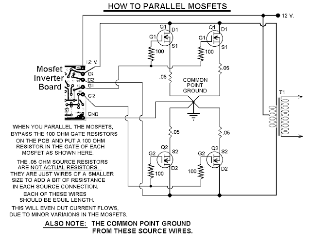
This 1000 watt power inverter circuit diagram based on MOSFET RF50N06.If you want more power then  add additional  MOSFET paralleled at RF50N06.This MOSFETS are  60 Volts and 50 Amps as rated.  It is necessary to connect  a  FUSE with the power line and always a LOAD have to connected while power is being  applied . The output power of this inverter is up-to 1k watt , it depends on output power transformer . You can use your custom transformer with experimenting for best result.

1000w
Fig: 1000 watt power inverter circuit diagram

How to parallel MOSFETs | 1000 watt power inverter


parallel
Fig-2: Parallel MOSFET Power Inverter


Circuit Credit: http://www3.telus.net/chemelec/Projects/Inverter/Mosfet-Inverter.htm

Thursday, November 6, 2014

Morning Alarm Circuit Diagram based LDR

This LDR based alarm can be used as get up alarm. The Alarm turns on in the morning automatically and turns off only when manually switched off ,so you will have to get up. It is a simple LDR based light sensor circuit.

LDR or Light Dependent Resistor is a kind of variable resistor and its resistance depends on the intensity of light falling on it. In complete dark, its resistance is as high as 1 Meg Ohm, but it reduces to 100 ohms or less in full light. So it is an ideal device to use as light switch. Sensitivity of LDR depends on its size also. Commonly available sizes are 3mm, 5mm, 10mm etc. But costly types with greater sensitivity are also available.

When the circuit is place in dark, near the window, LDR fails to conduct and T1 will not get base bias. So it remains off and buzzer will be silent. When the sunlight falls on LDR, IN the morning, LDR conducts and provides base bias to T1. T1 then conducts to activate the buzzer. Capacitor C1 is provided for the clean switching of T1. T1 will conduct only when C1 is charged fully. This prevents chirping sound during light transition.You can use an easily available Music buzzer to get melody tone.

Video Tracer Circuit Diagram

This circuit was designed as an aid to installers and maintainers of video systems. It is basically a video sync separator (IC1) followed by a LED and buzzer driver (IC2, Q1 & Q2). In use, the device is connected to a video cable and if there is video present, the LED will flash at about 10Hz. If there is no video, the LED flashes briefly every couple of seconds. A buzzer can also be switched in to provide an audible indication. The buzzer is particularly useful when tracing cabling faults or trying to find a correct cable amongst many, where it is difficult to keep an eye on the LED.

Another use for the buzzer option is to provide a video fault indication. For example, it could be inserted in bridging mode, with switch S1 in high impedance mode (position 2) across a video line and set to alarm when there is no video present. If someone pulls out a cable or the video source is powered off, the alarm would sound. IC1 is a standard LM1881 video sync separator circuit and 75Ω termination can be switched in or out with switch S1a. The other pole of the switch, S1b, turns on the power. The composite sync output at pin 1 is low with no video input and it pulses high when composite sync is detected.

Video Tracer Circuit diagram:

video

These pulses charge a 100nF capacitor via diode D1. When there is no video at the input, oscillator IC2b is enabled and provides a short pulse every couple of seconds to flash the LED. The duty cycle is altered by including D2, so that the discharge time for the 10μF capacitor is much shorter than the charge time. The short LED pulse is used as a power-on indicator drawing minimal average current. When video is present at the input, IC2b is disabled and IC2d is enabled. The output of IC2d provides a 10Hz square wave signal to flash the LED. The buzzer is controlled by switch S2. In position 2 the buzzer will sound when there is video at the input and in position 1 the buzzer will sound when there is no video at the input.


Sunday, November 2, 2014

SCAN TOOL OBD II INTREPRETER MODULE ELACTRONIC DIAGRAM

SCAN TOOL OBD-II INTREPRETER MODULE ELACTRONIC DIAGRAM

The interface is fully compatible with the popular ELM327 command set and supports all legislated OBD-II communication protocols, as well as the heavy-duty SAE J1939. It features automatic protocol detection, a large memory buffer, a UART interface capable of speeds of up to 10 Mbps, and a bootloader for easy firmware updates. The microOBD draws less than 1 mA in Standby mode, which makes it suitable for permanent in-vehicle installations. The host can force the module to enter the lowpower state by sending it an explicit “sleep” command or pulling the digital “host present” pin low. The module can also put itself in Standby automatically on UART inactivity or by sensing that the engine is off. Typical applications include diagnostic scan tools, code readers, data loggers, digital dashboards, fleet management, and vehicle tracking.

MXR Distortion plus schematic diagram

for subtly different sounds try replacing d1 + d2 with 1n34s for fuzzy sounds , 1n4148 for more buzz , leds for more crunch or a 1n34.
the original diodes were germanium 1n270 types.
components connected by dotted lines signify modifications for click prevention (1m resistor ) and osillation (cap in feedback  loop )

effect could be improved with true bypass switching .

Saturday, November 1, 2014

Wiring diagram 1995 Volvo 850 non Turbo

Wiring diagram 1995 Volvo 850 non Turbo The GLT BADGE returned for the 1995 model year, so now have versions of the 850 sedan, and station wagon 850 GLT, 850 Turbo, and 850 T-5R. T-5R is a model with more power stemming from ECU tuning and special suspension and wheels, spoilers. In addition to the introduction of the T-5R changes include new lamps for this type, option for side airbags, new internal switch gear design and a few other small changes (Wikipedia).


Here Wiring diagram 1995 Volvo 850 non Turbo

Friday, October 31, 2014

Pulse Generator And Signal Tracer Circuit Diagram

Dual-purpose test-instrument, Very simple circuitry, 1.5V Battery-operated. This simple circuit generates narrow pulses at about 700-800Hz frequency. The pulses, containing harmonics up to the MHz region, can be injected into audio or radio-frequency stages of amplifiers, receivers and the like for testing purposes. A high-pitched tone can be heard from the speaker of the device under test when all is working properly. The clip must be connected to the ground of the device under test, touching with the probe the different stages of the circuit, starting from the last stage and going up towards the first. When the tone is no longer heard, the defective stage has been found.

Connecting an earclip or headphone to J1, the circuit will automatically change into a two-stage amplifier and any audio signal coming from the device under test and picked-up by the probe will be heard through the headphones. The testing of a circuit should be made in the reverse manner, i.e. starting from the first stage and going down until the last stage. When nothing is heard, the defective stage has been found.

Circuit diagram:
Pulse
Pulse Generator And Signal Tracer Circuit Diagram


Parts:
R1________________1M 1/4W Resistor
R2,R4_____________2K7 1/4W Resistors
R3________________150K 1/4W Resistor
C1________________2n2 630V Ceramic or Polyester Capacitor (See Notes)
C2,C3_____________4n7 63V Ceramic or Polyester Capacitors
D1_______________1N4148 75V 150mA Diode
Q1_______________BC547 45V 100mA NPN Transistor
Q2_______________BC557 45V 100mA PNP Transistor
SW1______________SPST miniature Slider Switch (See Notes)
J1_______________Stereo switched 3mm. Jack socket (See Notes)
Probe____________Metal Probe 3 to 5 cm. long
Clip______________Miniature Crocodile Clip
B1_______________1.5V Battery (AA or AAA cell etc.)

Circuit operation:

Q1 & Q2 form a complementary astable multivibrator, whose operating frequency is set mainly by R3, C2 & C3 values. Output pulses are taken at Q2 Collector and applied to the probe by means of decoupling capacitor C1. D1 provides a symmetrical shape for the output waveform. If an earclip or headphone jack is plugged into J1, the connection from Q2 Collector and C1 - C2 is broken by the switch incorporated into J1: in this case the circuit becomes a two-stage amplifier.

Notes:
  • If you intend to use the circuit to test valve operated devices C1 must be a 630V type. Working with low voltage supply transistor devices the voltage of C1 can be lowered to 63 or 100V.
  • If instead of a short probe, you intend to connect the circuit to the device under test by means of a piece of wire longer than a few centimeters, a small ceramic capacitor (470 to 1000pF) should be added in parallel to D1 to prevent unwanted RF oscillation.
  • Current drawing when in Pulse-Generator mode is about 60µA and 1.2mA when in Signal-Tracer mode operation. Therefore SW1 can be omitted, provided that the earclip or headphones are unplugged when the circuit is unused.
  • J1 is a stereo switched jack socket wired to obtain a series connection of the two earpieces forming a stereo headphone. In this manner the circuit is loaded with a higher impedance and sensitivity will be improved.
  • Therefore, the higher the load impedance the more sensitive the Signal-Tracer. In any case, common 32 Ohm impedance mini-headphones suitable for walkman sets will work fine.
  • A crystal (high impedance) earpiece is a good solution, provided you substitute J1 with a mono switched jack socket.
  • The entire circuit can be easily fitted into a pen-like enclosure, with the probe protruding like a nib.

Thursday, October 30, 2014

Fastest Finger First Indicator Circuit Diagram

Quiz-type game shows are increasingly becoming popular on tale vision these days. In such games, fastest finger first indicators (FFFIs) are used to test the player’s reaction time. The player’s designated number is dis played with an audio alarm when the player presses his entry button. The circuit presented here determines as to which of the four contestants first pressed the button and locks out the remaining three entries. Simultaneously, an audio alarm and the correct decimal number display of the corresponding contestant are activated. 

Fastest Finger First Indicator Circuit Diagram:


Fastest Finger First Indicator Circuit Diagram
 
When a contestant presses his switch, the corresponding output of latch IC2 (7475) changes its logic state from 1 to 0. The combinational circuitry comprising dual 4-input NAND gates of IC3 (7420) locks out subsequent entries by producing the appropriate latch-disable signal. Priority encoder IC4 (74147) encodes the active-low input condition into the cor responding binary coded decimal (BCD) number output. The outputs of IC4 after inversion by inverter gates inside hex inverter 74LS04 (IC5) are coupled to BCD-to-7-segment decoder/display driver IC6 (7447). The output of IC6 drives common-anode 7-segment LED display (DIS.1, FND507 or LT543). 

The audio alarm generator comprises clock oscillator IC7 (555), whose output drives a loudspeaker. The oscillator frequency can be varied with the help of preset VR1. Logic 0 state at one of the outputs of IC2 produces logic 1 input condition at pin 4 of IC7, thereby enabling the audio oscillator.  IC7 needs +12V DC supply for sufficient alarm level. The remaining circuit operates on regulated +5V DC supply, which is obtained using IC1 (7805). Once the organiser identifies the contestant who pressed the switch first, he disables the audio alarm and at the same time forces the digital display to ‘0’ by pressing reset pushbutton S5. With a slight modification, this circuit can accommodate more than four contestants. 


Author : P. Rajesh Bhat  – Copyright : EFY

Friday, October 17, 2014

Simple Cmos Motorcycle Alarm Circuit Diagram

This Simple Cmos Motorcycle Alarm Circuit Diagram features an intermittent siren output and automatic reset. It can be operated manually using a key-switch or a hidden switch; but it can also be wired to set itself automatically when you turn-off the ignition. By adding external relays you can immobilize the bike - flash the lights etc.

Cmos Motorcycle Alarm Schematic Diagram

Cmos

Notes
Any number of normally-open switches may be used. Fit "tilt" switches that close when the steering is moved or when the bike is lifted off its side-stand or pushed forward off its centre-stand. Use micro-switches to protect removable panels and the lids of panniers etc.

Once activated - the rate at which the siren switches on and off is controlled by R9 & C5. For example - increasing the value of C5 will slow it down - while reducing the value of R9 will make it faster.

While at least one switch remains closed the siren will sound. About thirty seconds after all of the switches have been opened, the alarm will reset. How long it takes to switch off depends on the characteristics of the actual components used. You can adjust the time to suit your requirements by changing the value of R6 and/or C4.

The circuit is designed to use an electronic Siren drawing 300 to 400mA. Its not usually a good idea to use the bikes own Horn because it can be easily located and disconnected. However, if you choose to use the Horn, remember that the alarm relay is too small to carry the necessary current. Connect the coil of a suitably rated relay to the "Siren" output. This can then be used to sound the Horn - flash the lights etc.

The circuit board and switches must be protected from the elements. Dampness or condensation will cause malfunction. Connect the 1-amp in-line fuse AS CLOSE AS POSSIBLE to your power source. This is VERY IMPORTANT. The fuse is there to protect the wiring - not the alarm. Exactly how the system is fitted will depend on the make of your particular machine - so Im unable to provide any further help or advice in this regard.

The quiescent (standby) current of the circuit is virtually zero - so there is no drain on the battery. If you want to operate the alarm manually use a key-switch or a hidden switch connected to the "off/set" terminals. For automatic operation connect a wire from the ignition circuit to the "ignit" terminal. Then every time you turn-off the ignition - the alarm will set itself. Remember that this wire from the ignition switch is not protected by your 1-amp inline fuse. So unless its run is very short - fit the wire with its own 1-amp fuse as close as possible to its source.

When you set the alarm - if one of the switches is closed - the siren will sound. This could cause annoyance late at night. A small modification will allow you to Monitor The State Of The Switches using LEDs. When the LEDs are all off - the switches are all open - and its safe to turn the alarm on.

Veroboard Layout

Cmos


Thursday, October 16, 2014

100W Guitar Power Amplifier Circuit Diagram

The power amp board has remained unchanged since it was first published in 2002. It definitely is not broken, so there is no reason to fix it. The picture below shows a fully assembled board (obtainable as shown as M27). Using TIP35/36C transistors, the output stage is deliberately huge overkill. This ensures reliability under the most arduous stage conditions. No amplifier can be made immune from everything, but this does come close.

100W

Guitar Power Amplifier Board

The power amp (like the earlier version) is loosely based on the 60 Watt amp historically in the past published (Project 03), but its increased gain to match the preamp. Other modifications include the short circuit protection - the tiny groups of parts next to the bias diodes (D2 and D3). This new version is not massively different from the original, but has adjustable bias, and is designed to provide a "constant current" (i.e. high impedance) output to the speakers - this is achieved using R23 and R26. Note that with this arrangement, the gain will change depending on the load impedance, with lower impedance giving lower power amp gain. This is not a controversy, so may safely be ignored.

Ought to the output be shorted, the constant current output characteristic will provide an preliminary level of protection, but is not foolproof. The short circuit protection will limit the output current to a comparatively safe level, but a sustained short will cause the output transistors to fail if the amp is driven hard. The protection is designed not to operate under normal conditions, but will limit the peak output current to about 8.5 Amps. Under these conditions, the internal fuses (or the output transistors) will probably blow if the short is not detected in time.

Figure 2 - Power Amplifier

Figure two shows the power amp PCB parts - except for R26 which doesnt mount on the board. See Figure 1B to see where this ought to be physically mounted. The bias current is adjustable, & ought to be set for about 25mA dormant current (more on this later). The recommendation for power transistors has been changed to higher power devices. This will give improved reliability under sustained heavy usage.

As shown, the power transistors will have an simple time driving any load down to four ohms. In case you dont use the PCB (or are happy to mount power transistors off the board), you can use TO3 transistors for the output stage. MJ15003/4 transistors are high power, & will run cooler because of the TO-3 casing (lower thermal resistance). Watch out for counterfeits though! Theres plenty of other high power transistors that can be used, & the amp is tolerant of substitutes (as long as their ratings are at least equal to the devices shown). The PCB can accommodate Toshiba or Motorola 150W flat-pack power transistors with relative ease - in case you desired to go that way. TIP3055/2966 or MJE3055/2955 may even be used for light or ordinary duty.

At the input finish (as shown in Figure 1B), there is provision for an auxiliary output, & an input. The latter is switched by the jack, so you can use the "Out" & "In" connections for an outside effects unit. Alternatively, the input jack can be used to connect an outside preamp to the power amp, disconnecting the preamp.

The speaker connections permit up to 8 Ohm speaker cabinets (giving four Ohms). Do not use less than four ohm lots on this amplifier - it is not designed for it, & wont give reliable service!

All the low value (i.e. 0.1 & 0.22 ohm) resistors must be rated at 5W. The 0.22 ohm resistors will get warm, so mount them away from other parts. Needless to say, I recommend using the PCB, as this has been designed for optimum performance, and the amp gives an excellent account of itself. So nice in fact, that it may even be used as a hi-fi amp, and it sounds excellent. In case you were to make use of the amp for hi-fi, the bias current ought to be increased to 50mA. Ideally, you would use better (faster / more linear) output transistors as well, but even with those specified the amp performs well indeed. This is largely because they are run at comparatively low power, and the extreme non-linearity effects would expect with only transistors do not occur because of the parallel output stage.

Make positive that the bias transistor is attached to of the drivers (the PCB is laid out to make this simple to do). A some quantity of heat sink compound as well as a cable tie will do the job well. The diodes are there to protect the amp from catastrophic failure ought to the bias servo be incorrectly wired (or set for maximum current). All diodes ought to be 1N4001 (or 1N400? - anything in the 1N400x range is fine). A heat sink is not needed for any of the driver transistors.

The life of a guitar amp is a hard, and I recommend that you use the largest heat sink you can afford, since it is common to have elevated temperatures on stage (chiefly due to all the lighting), and this reduces the safety margin that normally applies for domestic equipment. The heat sink ought to be rated at 0.5° C/Watt to permit for worst case long term operation at up to 40°C (this is not unusual on stage).

Make sure that the speaker connectors are isolated from the chassis, to keep the integrity of the earth isolation parts in the power supply, & to make sure that the high impedance output is maintained.

Simple Frequency to Vvoltage Converter Circuit Diagram

This is Simple Frequency to Vvoltage Converter Circuit Diagram. In these applications, a pulse input at % is differentiated by a C-R network and the negative-going edge at pin 6 causes the input comparator to trigger the timer circuit. Just as with a V-to-F converter, the average current flowing out of pin 1 is IaverAGE = i (1.1 RjC^ f. 

In this simple circuit, this current is filtered in the network RL = 100 k ohm and 1 µF. The ripple will be less than 10 mV peak, but the response will be slow, with a 0.1 second time constant, and settling of 0.7 second to 0.1%.


Simple Frequency to Vvoltage Converter Circuit Diagram

Wednesday, October 15, 2014

Temperature Sensor Circuit Diagram

The LM35 temperature sensor provides an output of 10 mV/C for every degree Celsius over 0C. At 20C the output voltage is 20 10 = 200 mV. The circuit consumes 00. The load resistance should not be less than 5 kQ. A 4- to 20-V supply can be used.

Temperature Sensor Circuit Diagram

Temperature

Atv Jr Transmitter 440Mhz Circuit Diagram

This low-power video transmitter is useful for R/C applications, surveillance, or amateur radio applications. Seven transistors are used in a crystal oscillator-multiplier RF power amplifier chain, and a high-level video modulator. A 9- to 14-Vdc supply is required. Output is 0.4 to 1.2 W, depending on supply voltage. 


Atv Jr Transmitter 440Mhz Circuit Diagram

Atv

Monday, October 6, 2014

Circuit diagram License LGPL


Today younger brother generation that study same college comes to see at a house and beg to seek design good circuit and free. I advises a program TindyCAD because it drawing circuit diagrams commonly known as schematic drawings. It supports model the equipment is a lot of and still apply to PCB layout programs change the system netlist formats. Besides still be usable cooperate SPICE simulation netlists get as well. About the copyright be model freedom License LGPL be usable get freely model open source.

Wednesday, October 1, 2014

Active Crossover Circuit


This alive Cantankerous over is adequately beeline forward. It consists of a absorber and two 3rd order, 18 dB per octave filters. One low canyon and the added high. The cantankerous overabundance is set at 2Khz and is advised for AEK’s 400watt per access PA/Keyboard Amp systems. Obviously alone one access is apparent here.
The band akin audio arresting enters the absorber area it is astern out of phase. This is to atone for 
the filters which will alter the appearance afresh appropriately abiding the arresting to it’s able phase. The filters are more-or-less accepted low and aerial canyon filters appropriately however, added capacitors and resistors accept been added in adjustment to get the altruism bottomward to a minimum appliance alone E12 components.
This ambit may not be of awfully abundant use to anyone as it was accurately advised to clothing the applications. It is not capricious or switchable for two reasons. Firstly, it didn’t charge to be back the backdrop of the apostle arrangement were already known. And secondly, the added complication was put into the accurateness of the crossover rather than it’s flexibility. The filters are akin in account to anniversary added as able-bodied as can be accepted appliance alone E12 components. If switching were to be active to accord a ambit of abundance options, aaccommodation would accept to be fabricated on clarify accuracy.
The alone added way to accomplish a accepted crossover architecture and advance accurateness would apparently be to use Switched capacitor clarify architecture blocks. In theory, two 18or 24dB per octave filters could be complete such that they tracked anniversary added by actuality bound to the aforementioned clock. This would be a nice agreement but I haven’t had the befalling to prove this technology for this affectionate of application. My primary affair was the breach through of switching babble appliance such a design.
Therefore this architecture represents the simplest access I could booty and still get the adapted outcome.

Saturday, September 20, 2014

Driver’s Side Fuse Box Diagram Of Hyundai Santa Fe 2010

Driver’s Side Fuse Box Diagram Of Hyundai Santa Fe 2010
Circuit  guide   about Fuse Box Diagram Of 2002 Kia Optima. The parts fuse panel consist of: Instrument Cluster, Rear Wiper Relay, Rear Wiper Motor, Multifunction Switch (Wiper), Burglar Alarm Relay, Power Window Main Switch, Rear Power Window Switch LH, Power Window main Switch, Passenger Power Window,  Blower Relay, GM02 (Ground), Home Link, AC Inventer Module, Center Power Outlet, Front Power Outlet & Cigarette Lighter, Rear Power Outlet, Front Power Outlet & Cigarette Lighter, Door Lock/Unlock Relay, ICM Relay Box (Key Lock/Unlock Relay), Rheostat, BCM,Instrument Cluster (MICOM), AC Inventer Switch, AC Inventer Module, Audio, A/V & Navigation Head Unit, BCM, DVD Module, Digital Clock & Telltail, SRS Control Module, PODS Module, Instrument Cluster (IND), Drive/Passenger Door Lamp, Driver/Passenger Seat Warmer Control Module, Hazard Relay, Hazard Switch, BCM, Instrument Cluster (IND), Multifunction Switch (Light), Rear Combination Lamp (OUT) LH/RH, Head Lamp LH/RH, Driver/Passenger Vanity Switch, A/C Control Module, Cluster Ionizer, Incar Sensor, Sunroof Motor, Electro Chromic Mirror, Instrument Cluster (IND), BCM, A/V & Navigation Head Unit, Tire Pressure Monitoring Module, DVD Module, Tire Pressure Monitoring Module, A/C Control Module, BCM, Digital Clock & Telltail, Audio, A/V & Navigation Head Unit, DVD Module, Sport Module Switch, Key Solenoid, Altenator, Driver/Passenger Door Lock/Unlock Actuator, Tail Gate Lock Actuator,

25W Class A Power Audio Amplifier Wiring diagram Schematic

This is the 25W Class-A power audio amplifier schema. The output devices are MJL4281A (NPN) and MJL4302A (PNP), and have high bandwidth, fantastic SOA (safe operating area), high linearity and high gain. Driver transistors are MJE15034 (NPN) and MJE15035 (PNP). All devices are rated at 350V, using the power transistors having a 230W dissipation and the drivers are 50W.

25W Class-A Power Audio Amplifier Circuit Diagram

Build


  •  The supply voltage must be a maximum of ±25V. This supply is simply obtained from a 20-0-20V transformer, recommended current is 1A.
  •  All resistors ought to be 1/4W or 1/2W 1% metal film for lowest noise, with the exception of R9, R10 and R15 which ought to be 1/2W varieties, and R13, R14 have to be 5W wirewound.
  •  Using the suggested and advised 25V supplies, Q4 will typically not need a heatsink. The output drivers (Q5 and Q6) recommended to use a heatsink, even though it doesn’t have to be big.

Fuse Box F250 2008 Ford Superduty 4WD Diagram

Fuse Box F250 2008 Ford Superduty 4WD Diagram - Here are new post for Fuse Box F250 2008 Ford Superduty 4WD Diagram.

Fuse Box F250 2008 Ford Superduty 4WD Diagram


Fuse Panel Layout Diagram Parts: blower motor relay, low to hi relay, heated mirror, A/C clutch relay, PCM power relay, starter relay, trailer tow relay, park lamp, trailer tow relay battery charger, run start relay, fuel pump motor diode, A/C clutch diode, stoplamp, trailer tow relay, reversing lamp relay, fuel pump relay.

Friday, September 19, 2014

Fuse Box Ford 2006 SUV Diagram

Fuse Box Ford 2006 SUV Diagram - Here are new post for Fuse Box Ford 2006 SUV Diagram.

Fuse Box Ford 2006 SUV Diagram


Fuse
Fuse

Fuse Panel Layout Diagram Parts: trailer tow park lamp, park lamp, ignition switch, powertrain control module, fuel pump relay, main fan relay, passive anti theft system, high mounnted stop lamp, stop lamp, powertrain control module, brake pedal position switch, instrument cluster, diagnostic connector, power mirror switch, audio unit, canister vant, power seats, sunroof, compass, radio, power window, suwoofer, low eams, horn.

Thursday, September 18, 2014

Fuse Box Ford 1989 Ranger Two Wheel Drive Diagram

Fuse Box Ford 1989 Ranger Two Wheel Drive Diagram - Here are new diagram for Fuse Box Ford 1989 Ranger Two Wheel Drive Diagram.

Fuse Box Ford 1989 Ranger Two Wheel Drive Diagram


Fuse
Fuse

Fuse Panel Layout Diagram Parts: headlamp, park horn, marker and turn signal, posiion battery cable, starter relay, cutout relay, distribution box, power relay, pump relay, test connection, power convenience group.