Showing posts with label for. Show all posts

Wednesday, November 12, 2014

Booster for Input Impedance Circuit and explanation

The input impedance of a.c.-coupled op amp circuits depends almost entirely on the resistance that sets the d.c. operating point. If CMOS op amps are used, the input is high, in current op amps up to 10 MΩ. If a higher value is needed, a bootstrap may be used, which enables the input impedance to be boosted artificially to a very high value. In the diagram, resistors R1 plus R2 form the resistance that sets the d.c. operating point for opamp IC1. If no other actions were taken, the input impedance would be about 20 MΩ. However, part of the input signal is fed back in phase, so that the alternating current through R1 is smaller. The input impedance, Zin, is then: Zin=(R2+R3)/R3)(R1+R2). With component values as specified, Zin has a value of about 1GΩ. The circuit draws a current of about 3 mA.Circuit diagram:Input
Input Impedance Booster Circuit Diagram

Monday, November 3, 2014

Low Cost Playback Amplifier For Cassette Deck

For some time now, there have been a number of tape cassette decks available at low prices from mail order businesses and electronics retailers. Such decks do not contain any electronics, of course. It is not easy to build a recording amplifier and the fairly complex magnetic biasing circuits, but a playback amplifier is not too difficult as the present one shows.

 The stereo circuits in the diagram, in conjunction with a suitable deck, form a good-quality cassette player. The distortion and frequency range (up to 23 kHz) are up to good standards. Moreover, the circuit can be built on a small board for incorporation with the deck in a suitable enclosure. Both terminals of coupling capacitor C1 are at ground potential when the amplifier is switched on.

 Cassette Deck Playback Amplifier Circuit Diagram:


Because of the symmetrical ±12 V supply lines, the capacitor will not be charged. If a single supply is used, the initial surge when the capacitor is being charged causes a loud click in the loudspeaker and, worse, magnetizes the tape. The playback head provides an audio signal at a level of 200–500 mV. The two amplifiers raise this to line level, not linearly, but in accordance with the RIAA equalization characteristic for tape recorders. Broadly speaking, this characteristic divides the frequency range into three bands:
  • Up to 50 Hz, corresponding to a time constant of 3.18 ms, the signal is highly and linearly amplified.
  • Between 50 Hz and 1.326 kHz, corresponding to a time constant of 120 µs, for normal tape, or 2.274 kHz, corresponding to a time constant of 70 µs, for chromium dioxide tape, the signal is amplified at a steadily decreasing rate.
  • Above 1.326 kHz or 2.274 kHz, as the case may be, the signal is slightly and linearly amplified. This characteristic is determined entirely by A1 (A1’). To make the amplifier suitable for use with chromium dioxide tape, add a double-pole switch (for stereo) to connect a 2.2 kΩ resistor in parallel with R3 (R3’). The output of A1 (A1’) is applied to a passive high-pass rumble filter, C3-R5 (C3’-R5’) with a very low cut-off frequency of 7 Hz. The components of this filter have exactly the same value as the input filter, C1-R1 (C1’-R1’). The second stage, A2 (A2’) amplifies the signal ´100, that is, to line level (1V r.m.s.).

Monday, September 15, 2014

Noise Suppression For R C Receivers

Receiver interference is hardly an unknown problem among model builders. Preventive measures in the form of ferrite beads fitted to servo cables are often seen in relatively large models and/or electrically driven models, to prevent the cables from acting as antennas and radiating interference to the receiver. If miniature ferrite beads are used for this purpose, the connector must be first be taken apart, after which the lead must be threaded through the bead (perhaps making several turns around the core) and then soldered back onto the connector. An interference source can also cause problems in the receiver via the power supply connection.


 The battery is normally connected directly to the receiver, with the servos in turn being powered from the receiver. The servos can draw high currents when they operate, which means they can create a lot of noise on the supply line. This sort of interference can be kept under control by isolating the supply voltage for the receiver from the supply voltage for the servos. All of these measures can easily be implemented ‘loose’ in the model, but it’s a lot nicer to fit everything onto a single small schema board. That makes everything look a lot tidier, and it takes up less space.


The schematic diagram is shown in Figure 1. Connectors K1–K8 are located at the left. They are the inputs for the servo signals, which are connected to the receiver by the servo leads. The outputs (K9–K16) are located on the right. That is where the servos are connected. Finally, the battery is connected to K17. Interference on the supply voltage line due to the motors and servos is suppressed by a filter formed by L10, R1, C1 and C2. L10 is a ferrite-core coil with an impedance of 2000 ohms at 30 MHz. In combination with C1 and C2, it forms a substantial barrier to interference in the 35-MHz R/C band.


Signals with frequencies close to the 10.4-MHz intermediate frequency (which is used in many receivers) are also effectively blocked by this filter. L9 filters out common-mode noise on the supply line for the servos, which effectively means that it prevents the supply lines to the servos from acting as antennas. Finally, high-frequency currents on the servo signals are filtered out by ferrite beads in order to limit the antenna effects of these connection lines.

Resistor:
  • R1 = 1Ω
Capacitors:
  • C1 = 100nF
  • C2 = 22pF
Miscellaneous:
  • L1-L8,L10 = ferrite inductor
  • L9 = common-mode coil
  • K1-K8 = servo cable
  • K9-K17 = 3-way SIL pinheader

Sunday, September 14, 2014

SW Converter for Digital AM Car Radio

SW Converter for Digital AM Car Radio Circuit Diagram This schema is purposely presented with many loose ends (not literally, of course) to stimulate experimenting with RF schemary at a small outlay. Looking at the schema diagram you may recognize a modified version of the SW Converter for AM Radios described elsewhere in this issue. The modifications were necessary to make the schema compatible with a digital rather than analogue AM car radio. The main difference between digital AM radios and their all-analogue predecessors is that tuning is in 9 kHz (some-times 4.5 kHz steps) in compliance with the international frequency allocation for the band. Obviously, that particular step size, desirable as it may be on MW, is a stumbling block if you want to use a digital AM receiver in combination with a frequency step-up converter for SW, where chaos reigns and there is no fixed step size. The first attempt was to make the crystal oscillator variable by about 5 kHz each way.
 
SW Converter for Digital AM Car Radio Circuit diagram :
SW
SW Converter for Digital AM Car Radio Circuit Diagram
 
Unfortunately, despite serious efforts, the crystal could not be pulled more than 1 or 2 kHz so another solution had to be found. After studying the NE/SA602/612 datasheet, it was found that a variable LC based oscillator was the best alternative. The schema worked after winding a resonant LC schema and adding a 0.1 µF series capacitor to block the DC component on pin 6 of the NE602 (612). When the tuning was found to be a bit sharp with the original capacitor, a simple bandspread (or fine tuning) feature was added by shunting the LC resonant schema with a lightly loaded 365 pF tuning capacitor (C10) which, like the main tuning counterpart, C8, was ratted from an old transistor radio. The tuning coil, L1, consists of 8 to 10 turns of 0.6-0.8mm dia. enamelled copper wire (ECW) on a 6-8 mm dia. former without a core. With this coil, frequency coverage will be from about 4 MHz to 12 MHz or so. Details on Tr1 may be found in the referring article.
 
Note that no tuning capacitor is used on the secondary — the input stray capacitance of the NE602 (612) does the trick. A BFO (beat frequency oscillator) was added to enable SSB (single sideband) signals to be received. The BFO built around T1 is simple, has a heap of output and is stable enough to hold an SSB signal for a few minutes without adjustment. The BFO frequency is tuned with C3. Tr2 is a ready-made 455 kHz IF transformer whose internal capacitor was first crushed and then removed with pliers. When S2 is closed the BFO output signal is simply superimposed on the NE602 (612) IF output to the MW radio. The converter should be built into a metal box for shielding. If you find that the BFO gives too much output, disconnect it as suggested in the schema diagram and let stray coupling do the work. Sensitivity, even on a 1-metre length of car radio aerial, is quite amazing. Bearing in mind that most of the major international SW broadcasting stations like Radio NHK Japan, Moscow, BBC etc.) generate enough power to make sure that you will hear them, it is still quite exciting to hear such signals for the first time on your car radio. 

Monday, September 8, 2014

Under voltage Indicator for Battery Equipment Wiring diagram Schematic

This is the simple Under voltage Indicator for Battery Equipment Circuit Diagram. Due to the low duty cycle of flashing LED, the average current drain is 1 mA or less. The NE555 will trigger the LED on when the monitored voltage falls to 12 volts.The ratio of Rl to R2 only needs to he changed if it is desired to change the voltage point at which the LED is triggered.


Under voltage Indicator for Battery Equipment Circuit Diagram


Under

Temperature Monitor for Electronic Equipment

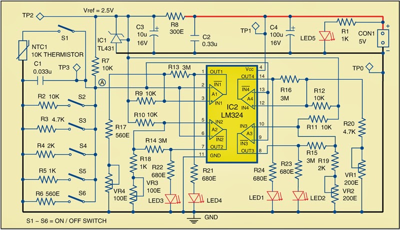
Build a Temperature Monitor for Electronic Equipment schema diagram. As most electronics components’ characteristics vary with temperature, they are selected as per expected operating temperature range of the equipment. So it is important that the equipment stays within the temperature range for which it is designed.


This schema warns when the temperature reaches predefined danger levels. Here the predefined levels are set to 45°C, 65°C, 85°C and 105°C, but one can set any other temperature levels to suit the equipment in use.Circuit and workingFig. 1 shows the temperature monitoring schema. It is built around 10k NTC thermistor NTC1, shunt regulator TL431 (IC1), popular comparator LM324 (IC2) and some other components.

 Temperature Monitor for Electronic Equipment Circuit Diagram

 temperature monitor for electronic equipment


IC2 activates corresponding LEDs (LED1 through LED4) when the temperature of thermistor NTC1 reaches the predefined level (refer Table I). The temperature is sensed by NTC1 and the produced corresponding voltage at point ‘A’ is fed to inverting terminal of all the four op-amps (A1 through A4). Switch S1 should be closed for this operation. This voltage level is compared with the reference voltage at non-inverting terminals of each op-amp. The reference voltage is obtained by voltage dividers from 2.5V reference source, which is produced using shunt regulator IC1. The reference voltage for each comparator can be set using presets VR1 through VR4.

http://streampowers.blogspot.com/2014/02/temperature-monitor-for-electronic.html

http://streampowers.blogspot.com/2014/02/temperature-monitor-for-electronic.html


The switches S2 through S6, together with resistors R2 through R6, are used for calibration purpose. For example, op-amp A4 of IC2 compares the voltage levels at point A (changing with change in temperature) with the reference voltage at its pin 12. The voltage level at pin 12 of A4 is adjusted with preset VR1. Switches S2 through S6 are used to simulate voltage levels corresponding to different temperatures.A4 is tuned for 45°C by keeping switch S3 in closed position and trimming preset VR1 until LED1 glows. S1 should be open during calibration. The same procedure is repeated for comparator A3, A2 and A1 to tune them for 65°C, 85°C and 105°C. Table I shows the presets and LEDs corresponding to each temperature level. After calibration, open switches S2 through S6.


Sourced By : EFY Author: Petre Tzv. Petrov

Sunday, September 7, 2014

Most Power Supply for Amplifier


Power supply
As with most power amplifiers, the ±60 V power supply need not be regulated. Owing to the relatively high power output, the supply needs a fairly large mains transformer and corresponding smoothing capacitors—see circuit diagram below.

Most
Note that the supply shown is for a mono amplifier; a stereo outfit needs two supplies. 

The power supply is straightforward, but can handle a large current. Voltage acserves as drive for the power-on delay circuit. The transformer is a 625 VA type, and the smoothing capacitors are 10 000 µF, 100 V electrolytic types. The bridge rectifier needs to be mounted on a suitable heat sink or be mounted directly on the bottom cover of the metal enclosure.. The transformer needs two secondary windings, providing 42.5 V each. The prototype used a toroidal transformer with 2x40 V secondaries. The secondary winding of this type of transformer is easily extended: in the prototype 4 turns were added and this gave secondaries of 2x42.5 V.

Friday, September 5, 2014

Amplifier for Paralelling Headphone

Amplifier
The circuit is useful to strengthen the voice on the headphones, which is where the headphones have a stereo output is used and paralleled to some headphones. The circuit is based on the TDA2822 amplifier circuit modified to ampifier headphones.


Amplifier
Amplifier for Paralelling Headphone
In the amplifier circuit I do not put potensio meter to adjust the size of the desired sound on headphones, I just give constraints on two 33K resistors so that the voice issued not too hard. But if you want to make the sound volume settings, you can replace the 33K resistor with potensio meters or trimpot with resistance at 50K. Input voltage in the circuit I took it from a usb DVD, PC, which berkeluaran voltage 5 V DC, which can supply chain so it can work with the good. To parallel his headphones can be seen below...

Paralel
Paralel Headphone Wiring Diagram

Friday, August 29, 2014

XM Satellite Radio Vs Sirius for your Auto Sound System Selection

If youre in the market for a new auto sound system you might want to seriously take a moment and consider whether or not you would be benefited by subscribing to either Sirius or XM Satellite Radio. Both of these subscription-based services have something wonderful to offer their subscribers and both of them require specialized equipment in order to operate. This means if you are going to wish to use either service, you will need to have decided which service before you have your auto sound system installed.


XM
It really doesnt matter which of these you choose they each have different features that will appeal to a wide variety of audiences. You will find some wonderful competition among the two not only by way of music radio but also talk radio. If you really love talk radio you really need to subscribe to one of these in order to find a treasure chest of talk radio gems. You will find everything from the mundane to the controversial. From Oprah to Howard Stern exist in the realm of satellite radio, which seems to not only be catching on but also here to stay.

It has been commented on many times that XM Satellite Radio has a strong lead when it comes to subscriptions. This is very true but you should also keep in mind that the new subscribers seem to be leaning more towards Sirius for their satellite radio rather than going with the traditional favorite. Ive checked out the line up and cant see that one has much of a clearly defined lead over the other so I cant give a definitive reason for the massive new subscribers to Sirius or even the phenomenal lead that XM Satellite radio is currently enjoying. Regardless if this is something that might interest you, you really should check out each website and decide for yourself which, if either, is more appealing to you as well as whether that appeal is worth the investment and the monthly subscription fee.

I will say this however: XM Satellite Radio for the moment seems to have much better toys to offer consumers. That being said, Im actually quite surprised that the vast number of new subscribers are going with Sirius rather than XM. Of course, being the gadget geek that I am, I am basing that surprise solely on the fact that XM seems to have much better toys. At the moment XM is offering some really cool gadgets that double not only as XM Satellite Radio receivers but also offer GPS functionality and navigation assistance and controls. Some of these devices even go one step further and play DVDs, CDs, MP3s, among other things.

Believe me, Sirius has a lot to offer its customers as well, Im simply thrilled over select items that can be found at XM that I really havent seen adequate competition for elsewhere. On the level of music, both seem to carry similar genres, lineups, etc. The same holds true for the Talk radio line up. The only major difference I am finding between the two are the gadgets. Even the prices are rather competitive with one another. I see only one other major difference and that is the fact that Sirius offers a lifetime membership that cost about the same as the five-year plan from XM Satellite Radio. The thing to remember however is that the lifetime membership is for the lifetime of the device not the subscriber.

I should also point out that opting for satellite radio more than likely will not eliminate your need for a new auto sound system it may however pose certain requirements for the type of sound system you will be able to choose. One thing I have noticed with both companies is that there are plenty of devices from which to choose. You will have your hands full selecting the right equipment for your auto sound system upon which to enjoy the wonderful sounds that satellite radio will bring to your ears each and every day.

Wednesday, August 27, 2014

FM adaptor circuit for car stereo


With this compact FM adapter schema plugged into the audio out of your cassete player or i Pod out put,you can listen your favorite music on your car stereo.This schema is very useful if your car stereo does not have an auxiliary in socket.The schema is nothing buy an short range FM transmitter.


The FM transmitter schema is based on low power NPN transistor 2N2222.The tank schema consisting of L1 & C1 produces the necessary oscillations at the collector of Q1.The capacitance C4 , resistance R3 & R4 performs the function of mixing the stereo out put from the audio player or i-Pod.The emitter resistance R2 provides sufficient stability to the schema.It also limits the collector current to increase the battery life.


Notes.

* Use a 28SWG , 10 cm insulated copper wire as antenna.
* For L1.make 8 turns of 20 SWG insulated copper wire on a 5mm dia plastic former.
* Power the schema from a 3V battery.
* Assemble the schema on a good quality PCB or common board.
* C1 can be a 50pF trimmer.

Tuesday, August 26, 2014

Crossover For Subwoofer

The crossover network is intended for use when an existing audio installation is to be extended by the addition of a subwoofer. Often, this additional loudspeaker is one that has been lying around for some time. If its frequency response extends down far enough, all is well and good, but a filter is then needed to cut off any frequencies above, say, 150 Hz. Often, a subwoofer network is an active filter, but here this would necessitate an additional power supply. The present network is a passive one, designed so that the speaker signal of the existing system can be used as the input signal.

Crossover For Subwoofer Circuit diagram:

Crossover

 Crossover Circuit Diagram For Subwoofer

Since the bass information is present in both (stereo) loudspeakers, the signal for the sub woofer can simply be tapped from one of them. The network is a 1st order low-pass filter with variable input (P1) and presettable cut-off frequency (P2). The signal from the loudspeaker is applied to terminal ‘LSP’. Voltage divider R1-R2-P1 is designed for use with the output signal of an average output amplifier of around d 50 W. The crossover frequency of the network may be varied between 50 Hz and 160 Hz with P2. The values of R3, P2, and C1, are calculated on the assumption that the subwoofer amplifier to be connected to K1 has a standard input resistance of 47 kΩ.

If this figure is lower, the value of C1 will need to be increased slightly. It is advisable to open the volume of the subwoofer amplifier fully and adjust the sound level with P1. This ensures that the input of the subwoofer amplifier cannot be overloaded or damaged. Make sure that the ground of the loudspeaker signal line is linked to the ground of the subwoofer amplifier. If phase reversal is required, this is best done by reversing the wires to the subwoofer. If notwithstanding the above additional protection is desired at the input of the subwoofer amplifier, this is best effected by ‘overload protection ’ elsewhere in this site.

Author: T. Giesberts Copyright: Elektor Electronics

Monday, August 25, 2014

Best Amplifier for signal supply Wiring diagram Schematic

Best Amplifier for signal supply Circuit Diagram complicates the design process even further because of the reduced signal swings. This unity-gain follower amplifier has a CMOS p-channel input, an npn second-gain stage, and a CMOS inverter output. The IC building blocks are two CA3600E`s (CMOS transistor pairs) and a CA3046 npn transistor array. A zener-regulated leg provides bias for a 400-I`A p-channel source, feeding the input stage, which is terminated in an npn current mirror. 

 Best Amplifier for signal supply Circuit Diagram

Best

 The amplifier voltage-offset is nulled with the 10-K!l balance potentiometer. The second-stage current level is established by the 20-K!lload, and is selected to approximately theist-stage current level, to assure similar positive and negative slew rates. The CMOS inverter portion forms the final output stage and is terminated in a 2-K!l load, a typical value used with monolithic op amps. Voltage gain is affected by the choice of load resistance value. The output stage of this amplifier is easily driven to within 1 mV of the negative supply voltage.

Friday, August 22, 2014

zBot 10 A Power Stage for DC Motor Wiring diagram Schematic

zBot :10-A Power Stage for DC Motor Circuit Diagram . If you look at the chassis of the zBot vehicle1, you’ll find two parts requiring intelligent control: the steering servo and the DC motor. The so called H-bridge is the normal schema for electronic control of revolution speed and direction. The DC motor of a Tamiya car is powerful enough to propel zBot at up to 20 miles per hour.
.
The motor then consumes more than 10 A, so we choose high-current power MOSFETs for the driver stage. There are lots of different devices to choose from. The MOSFET we require has to supply the maximum motor current and, importantly, it has to be switched with gate voltages of about 5 V. In this case, the microcontroller switches the power stage (‘low side’) directly. For high side driving level shifters are necessary. The schematic of the H-bridge power stage shows a few inverters, NAND gates and two tri-stateable drivers. These logic functions are very important as the easier way, i.e.., directly controlling all four MOSFET has a fatal disadvantage.

zBot :10-A Power Stage for DC Motor Circuit Diagram

zBot


In case of a software crash it could happen that two ore more MOSFETs are switched on incor-rectly for exam-ple, T4 and T7. In that case, the current through the transistors is limited by the internal resistors of the MOSFETs (about 10 mO) only. Such a fatal error would destroy the MOSFETs. The logic functions configured here effectively avoid illegal states.To control the DC motor, three signals are needed: DIR, PWM and STOP. DIR controls the direction of the motor revolution, PWM the speed, and STOP brakes the motor.

The software module for the DC motor is called dcm.c.(070172-I) The complete document called Zbot  the Robot Experimental Platform is available for free downloading from the Elektor Electronics website. The file number is 070172-11.zip (July/August 2007).

Sourced by : Circuitsstream.blogspot.com

Monday, August 18, 2014

Portable CD Player Adapter For Car

Whenever Im in the car listening to my favourite CD, it always happens; my batteries go dead. To solve that problem, I built this extremely simple regulator schema. It steps down the 12V from the lighter socket to 9V which is used by the CD player. Different CD players (I have a Sony Discman) may require different voltages, so just use the correct regulator. All the 78xx series regulators have the same pin out, so the schema is universal.

Portable CD Player Adapter For Car Circuit daigram


Parts List

Part           Total Qty.                     Description

C1                      1                        1000uF 25V Electrolytic Capacitor   
C2                      1                        10uF 25V Electrolytic Capacitor   
C3                      1                        1uF 15V Elextrolytic Capacitor   
C4                      1                        0.1uF 15V Electrolytic Capacitor   
U1                      1                        7809 Or Other Regulator (See "Notes")    See Notes
MISC                  1                        Cigarette Lighter Plug, Plug For CD Player (See "Notes"),      Heat Sink For U1, Wire, Case.   
   
Notes
  • The voltage your CD player needs will determine which regulator you use. For 9V, use the 7809. For 6V, use the 7806. For the unlikely 5V use the 7805. Remember that whatever regulator you use, you will need to heat sink it. The metal case or metal cover on the case makes a great heat sink.
  • I built the schema in a small case with the long wire to the cigarette lighter plug coming out one end, then another, slightly shorter wire going out the other end to the CD player.
  • Triple check your wiring. You would hate to ruin an expensive CD player because you reversed one of the connections or hooked the regulator up backwards.