Showing posts with label power. Show all posts

Wednesday, November 19, 2014

Stereo Power Amplifier STA550

Stereo Power Amplifier 2x70Watt STA550 is chip audio power with BASH concept that can be connected with digital devices. 2x70Watt STA550 Stereo Power Amplifier is an amplifier with BTL system with symmetrical power supply with ground. Power amplifier STA550 uses power output transistor which is on the chip and is set to produce a high efficiency audio power. Power output on the STA550 is using the system without copling ac bridge (direct) and zero offset.

Strengthening of the STA550 from stereo power amplifier is +12 dB. 2x70Watt STA550 Stereo Power Amplifier is equipped with temperature sensors for protection from overheating and current-limiting protection system for power amplifier. 2x70Watt STA550 Stereo Power Amplifier is equipped with standby and mute controls to regulate silent or active mode power amplifier.


    Feature :

  •      Monochip Bridge Stereo Amplifier with Bash ® Architecture
  •      55 +55 w Output Power @ Rl = 4 / 8 W, THD = 0.5%
  •      70 +70 w Output Power @ Rl = 4 / 8 W, THD = 10%
  •      High Dynamic preamplifier Input Stages
  •      Programmable External Feedback Type Compressors
  •      AC Coupled Input Output Bridge To Class Ab Amplifier
  •     Precision Rectifiers To Drive The Digital Converter
  •      Proportional Over Power Output Current Limit To The Digital Converter
  •      Absolute Power Transistor Bridge Output Power Protection
  •      Absolute Output Current Limit
  •      Integrated Thermal Protection
  •      Power Supply Over-Voltage Protection Flexiwatt With 27 Pin Power Package
  •      Bash ® Licence Require

Sunday, November 16, 2014

Type of UPS Uninterruptible Power Supply

UPS design of the model is divided into several types that produce different performance characteristics:
A. Standby
2. Line Interactive
3. Double Conversion On-Line
4. Delta Conversion On-Line
Standby UPS types
This type is commonly used by home users for the Presidency with their PC. UPS to be able to do this type of filtration against power failures and flow management, in addition to design efficient, small size and inexpensive.

Line Interactive UPS types
UPS is the type most often used in small business unit, web developer, and a number of servers located in government departments. Because, in addition to having high levels of reliability, this type also have the ability to adjust the voltage that is sufficient
fine.
UPS has an inverter is always connected to the output of the UPS system to convert the power from batteries into AC. In normal circumstances, the Inverter will perform battery charging. While in a state of power outages, Transfer Switch will close and drain power from the batteries to the UPS output. Position that is always connected to the inverter output filter provides additional power. This makes the type of UPS is widely used for server and electrical conditions are not too good.

Double Conversion type UPS On-Line
This type is most common for UPS with power more than 10kVA. These types have in common with the type of Standby. Only this type has a power source located on the inverter, not the AC power source. In this type, the main electricity supply interruption will not trigger a transfer switch for the incoming AC power to the central input to charge the batteries that provide power to the Inverter located at the output. Therefore, when the AC power is disconnected, the flow of energy will be transferred immediately without taking a break when the transfer occurs. This type of UPS above shows the performance of the average. Can be said of this type of approach the ideal of a UPS, unfortunately this type of heat is high enough.

UPS type Delta Conversion On-Line
Almost the same as the Double Conversion type, type Delta used to always supply voltage Inverter. When the power supply is interrupted, this type do the same with Double Conversion type. Delta Conversion has two functions, the first is to control the input power characteristics. While the second function is to control the input current to direct the process of charging the battery system. The thing to remember is to minimize this type of energy is wasted. In addition, it has a high compatibility to various types of generators and reduce the need for the use of cables.

Friday, November 14, 2014

Booster Low Power Voltage Doubler Diagram Circuit

All miniature electronic devices operate off batteries. Some of them need higher than the standard battery voltages to operate efficiently. If the battery of that specific voltage is unavailable, we are forced to connect additional cells in series to step up the DC voltage. Thus, the true meaning of miniaturisation is lost. A simple way to overcome this problem is to employ a voltage doubler, if the device under consideration can operate at a small current.

Here we present a low-power voltage doubler circuit that can be readily used with devices that demand higher voltage than that of a standard battery but low operating current to work with. The circuit is quite simple as it uses only a few components. Yet, the output efficiency is 75 to 85 percent along its operating voltage range. The available battery voltage is almost doubled at the output of the circuit.

Here IC1 is wired as an astable multivibrator to generate rectangular pulses at around 10 kHz. This frequency and duty cycle of the pulses can be varied using preset VR1. The pulses are applied to switching transistors T1 and T2 for driving the output section, which is configured as a voltage-doubling circuit. The doubled voltage is available across capacitor C5. During each cycle of the pulse occurance, the high level drives T1 into its saturation, keeping transistor T2 cut off.Circuit diagram:
Low-Power Voltage Doubler Circuit Diagram

So transistor T1 charges capacitor C4 via the path formed by diodes D2 and D1 to a voltage level slightly lesser than the supply. But during the low period of the pulse, transistor T1 is cut off while transistor T2 is driven into saturation. Now, transistor T2 raises the charge on the negative pole of capacitor C4 by another step equal to the supply voltage. Therefore an equal amount of charging is built up on capacitor C5 via diode D3.

This doubling action increases the total voltage across capacitor C5 to almost double the input voltage. If the output of the pulse generator is maintained with a high enough amplitude and frequency, the output voltage and current remain constant and cater to the needs of the load. Even with the half-wave function, this circuit is almost free of ripple voltage. If the connected load doesn’t require a high current, the efficiency can be expected in the upper 90 percentranges.

Since the input voltage is doubled, the current drain from the input power supply is also doubled at the input but halved at the output. One point of caution is that if the multivibrator’s frequency is fairly high, the output may suffer with the interference imposed over the DC voltage. In this case, the frequency must be set favorably by trials and actual load connection procedure. This tiny circuit can be assembled on the general-purpose PCB. If all of the components are surface-mount type, the whole module can be genuinely miniaturized.EFY Lab note.
During testing with input of 8V and 1.25mA load current the output voltage was found to be around 13V.
Source: EFY Mag

Thursday, November 13, 2014

1000 watt power inverter circuit diagram

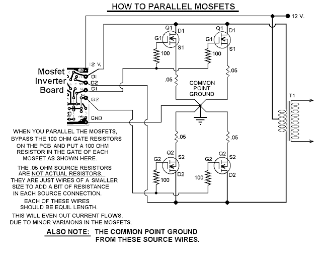
This 1000 watt power inverter circuit diagram based on MOSFET RF50N06.If you want more power then  add additional  MOSFET paralleled at RF50N06.This MOSFETS are  60 Volts and 50 Amps as rated.  It is necessary to connect  a  FUSE with the power line and always a LOAD have to connected while power is being  applied . The output power of this inverter is up-to 1k watt , it depends on output power transformer . You can use your custom transformer with experimenting for best result.

1000w
Fig: 1000 watt power inverter circuit diagram

How to parallel MOSFETs | 1000 watt power inverter


parallel
Fig-2: Parallel MOSFET Power Inverter


Circuit Credit: http://www3.telus.net/chemelec/Projects/Inverter/Mosfet-Inverter.htm

Tuesday, November 11, 2014

Photovoltaic Power System and Wiring Module Interconnection

Photovoltaic
Photovoltaic (PV) is the field of technology and research related to the application of solar cells for energy by converting sunlight directly into electricity. The following Photovoltaic Power System manual is a suggested practices manual examines the requirements of the 2005 National Electrical Code (NEC) as they apply to photovoltaic (PV) power systems. In this manual you will get the design requirements for the balance-of-systems components in a PV system are addressed, including conductor selection and sizing, overcurrent protection device rating and location, and disconnect rating and location.

This manual is divided into sections which covers discussion on Photovoltaic Modules (including Modules Marking, Wiring, Module Interconnection, Tracking Modules, Terminals, Transition Wiring, Module Connection Access, Module Connectors, and Splices), Conductor Color Code, PV Array Ground-Fault Protection, PV Array Installation and Service, Grounding (including size of DC grounding electrode conductor, point of connection, charge controller, ungrounded system), Equipment Grounding, Inverter AC Outputs, Conductor Ampacity, Overcurrent Protection, Batteries, Generators, Charge Controller, Inverters, Stand Alone Distribution System, etc.

Copper conductors are recommended for almost all photovoltaic system wiring. Copper conductors have lower voltage drops and better resistance to corrosion than other types of comparably sized conductor materials. Aluminum or copper-clad aluminum wires can be used in certain applications, but the use of such cables is not recommended—particularly in dwellings. All wire sizes presented in this guide refer to copper conductors.

Find more information about Photovoltaic Power System and Wiring Module Interconnection in the following manual. (source: scribd.com)

Wednesday, November 5, 2014

Spy Camera Solar Power Box

Battery life has always been a critical consideration for most of the electronic gadgets and equipment. When we talk about spy  cameras,  which  normally  function  round-the-clock, they often run out of power within a few days.  Many spy cameras (CCTV cameras) are powered by 9V PP3 type batteries that offer five times more energy  than the regular 9V alkaline battery.

Mini CCTV cameras also accept 6-12V DC supply from AC mains adaptor through the DC IN jack. AC mains adaptor for the camera increases the capacity of the 9V PP3 battery but is bulky and noisy. Whether disposable  or rechargeable batteries, making frequent replacement or recharging them is a cumbersome job. The unique solar power box described here serves an alternative solution to the problem. 

Spy Camera Solar Power Box Circuit diagram :

Spy

The circuit of the solar power box is simple. It contains a  battery charger and a battery health indicator and  a few other components.  As shown in the circuit,  DC supply available from  the solar panel (SP1) is  directly applied to the in-put of the circuit through  a protection diode (D1).  This diode is used to pre-vent  the  reverse  current  flow from the battery to  the  solar  panel  during  night. Thus, D1 allows  the current to flow from the solar panel  to the battery only. Low-voltage-drop  type 1N5817 diode is perfect for the  job.
At the heart of the circuit is an integrated current source, realised using a  popular 3-pin adjustable voltage regulator LM317T(IC1). 

This IC is designed  to adjust its internal resistance between  the In (pin 3) and Out (pin 2) terminals  to maintain a constant voltage of 1.25V  between the Out (pin 2) and Adj (pin 1) terminals. Here, a 9V, 280 mAh  rechargeable PP3 type Ni-MH battery  (BATT) is used as reservoir. Normally,  a charging current of about 10 per cent  of  ampere-hour  rating  is  safe  for  the  battery. Resistor R1 (39-ohm, 0.5W),  connected between pin 1 and 3 of IC1,  limits  the  charging  current  to  about  30 mA. DC output from the battery is  available at output jack J2. Red LED  ( LED1) is used as a battery ‘health’  indicator. Switch S1 is used to start the  charging while S2 is used for connect-ing the load. Note that suitable heat  sink should be used for the IC1.

The proper selection of solar panel  is important but not critical. A miniature 12V type solar panel with a cur-rent output of about 100 mA can be  used. Even if you have a solar panel  with  higher  voltage  rating,  it  will  not  create a problem as the circuit ensures  that the charging current cannot exceed  the predetermined value.

The circuit can be easily assembled  on a general-purpose PCB and housed  in a small plastic cabinet.


Thursday, October 30, 2014

Mosfet Amplifier 20Watt Output Power

This audio amplifier showed in this circuit diagram , is a very simple and efficiency audio amplifier circuit based on the TDA1308 integrated class-AB stereo headphone . The device is fabricated in a 1 mm Complementary Metal Oxide Semiconductor (CMOS) process and has been primarily developed for portable digital audio applications.

You can use this circuit diagram with TDA1308 or TDA1308A , the difference between the TDA1308 and the TDA1308A is that the TDA1308A can be used at low supply voltages. The maximum output power that can be obtained with this circuit is around 80mwatts. This audio amplifier circuit requires a very low voltage power supply : from 3 to 7 volts for single supply or 1.5 to 3 volts for dual supply , for TDA1308 .

The TDA1308A supports a low voltage input down to 1.2 volts , but the typical power supply required for both circuits is 5 volts for single supply and 2.5 volts for dual supply .

As you can see the circuit requires very few external components and can be configured to work in stereo or mono configuration.

Mosfet

Wednesday, October 29, 2014

20 Watt Power Amplifier Circuit

20
This IC hew was designed specifically used for bring into play trendy power boosting applications in automobiles. It is self caring aligned with petite circuits and thermal problems. In the conduit configuration given away it hope against hope provide 20 watts of power into a 2 ohm spokeswoman operating next to 14.4 volts.

Monday, October 27, 2014

9 Volt Audio Power Amplifier

This is an audio amplifier to facilitate can be there used with a miniature 9 volt Battery Operated,Current draw on since insufficiently as 5 milliamps.And amplification up to 500 mW. Which is sufficient to spread out the sound from a sound almost or else the recording stroll guy vetoed to the minor speakers evidently.

9 Volt Audio Power Amplifier
Once entering the power supply 9-volt circuit IC1 total LM386 amplifier IC size is 300-800 mW, Depending on the power supply circuit with,This is from 4-15 volts. once upon a time entered into the input pin 3,The non inverting pin to amplifier non-return time.C1 resolve occur served remove out the clatter input to ground.And C2 increases the rate of amplifier,C2 is to add supplementary help.But if the C2 Too much distortion (the C2 must not exceed 100uF).The output of IC1 is out cold of the pin 5 through C4 coupling audio signals to better and DC blockade and not voted for to the spokesperson.on behalf of the audio portion bidding besides befall fed back through R2 and C3 to the above what is usual frequency response better.

4 Channels Home Audio Power Amplifier

This is a minimal circuit. right management a single IC, but the amplifier has 4 channels, 11 channels apiece watt, which is Philips IC TDA1554 run to apposite in support of listening by the side of land of your birth otherwise dressed in one vehicle. Just since the power supply 12-15 volt otherwise yearn for transpire used to open out any home acting sound organization. The at the outset 2-channel amplifier front speakers. And 2 to widen the back surround sound speakers additionally.

4 Channels Home Audio Power Amplifier
This circuit power supply 12 volts to 18 volts Power consumption next to 5A. The input 4 input pins 1, 2, 17 and 18 is not speaking into a horizontal input inverter Ting 2 channels (Pin 1, 17). inverse classic and input object 2 channels (pins 2, 6). with the purpose of we can function that. To output point to phase or else did not return. The output self-control be there the fourth slot on the crutch 6, 8, 12, 10, with a C7-C10 serves to boost the low frequency stability better in the past you die to the loudspeaker. The switch S1 acts on mute by urgent S1 will be stopped sound procedure circuit here Mute, and if unfasten circuit S1 supply on the point of to masterpiece. The C5 and C6 bidding filter light to smooth absent and eliminate interference.

Friday, October 17, 2014

0 - 300V Adjustable Power Supply

0 - 300V Adjustable Power Supply


Introduction

To prevent my high voltage experiments to go up in smoke completely, I designed
a simple circuit which can provide an adjustable voltage source of 0 to 330 Volt..
The supply is short-ciruit proof: the current is limited to about 100mA.

Circuit description

TR1 is a 1:1 mains transformer; it is included for safety.

The mains voltage from TR1 is rectified with bridge D1 (1Amp / 500V) and large elcap C1.

T1 is switched as a source follower: the source of T1 will follow the voltage of the
wiper of R3. D2 is included to protect the gate of T1; although in theory not necessary
I strongly recommend to include it!

T2 and shunt resistor R2 build the current limiter. When the output current becomes too high, T2 will discharge
the gate of T1. This will prevent the current to become too high.
The value of R3 has been determined experimentally; it depends also on the Hfe of T2 so you may need to tune the value of R2.

Note that T1 needs a large heatsink: in worst case T1 will dissipate 330V x 100mA = 33Watt!
Instead of a BUZ 326 (400V/10.5Amp) you can also use an IRF740 (400V/10Amp).
The output impedance of the power supply is determined by the beta of T1, so the larger the MOSFET
the lower the output impedance!

Thursday, October 16, 2014

100W Guitar Power Amplifier Circuit Diagram

The power amp board has remained unchanged since it was first published in 2002. It definitely is not broken, so there is no reason to fix it. The picture below shows a fully assembled board (obtainable as shown as M27). Using TIP35/36C transistors, the output stage is deliberately huge overkill. This ensures reliability under the most arduous stage conditions. No amplifier can be made immune from everything, but this does come close.

100W

Guitar Power Amplifier Board

The power amp (like the earlier version) is loosely based on the 60 Watt amp historically in the past published (Project 03), but its increased gain to match the preamp. Other modifications include the short circuit protection - the tiny groups of parts next to the bias diodes (D2 and D3). This new version is not massively different from the original, but has adjustable bias, and is designed to provide a "constant current" (i.e. high impedance) output to the speakers - this is achieved using R23 and R26. Note that with this arrangement, the gain will change depending on the load impedance, with lower impedance giving lower power amp gain. This is not a controversy, so may safely be ignored.

Ought to the output be shorted, the constant current output characteristic will provide an preliminary level of protection, but is not foolproof. The short circuit protection will limit the output current to a comparatively safe level, but a sustained short will cause the output transistors to fail if the amp is driven hard. The protection is designed not to operate under normal conditions, but will limit the peak output current to about 8.5 Amps. Under these conditions, the internal fuses (or the output transistors) will probably blow if the short is not detected in time.

Figure 2 - Power Amplifier

Figure two shows the power amp PCB parts - except for R26 which doesnt mount on the board. See Figure 1B to see where this ought to be physically mounted. The bias current is adjustable, & ought to be set for about 25mA dormant current (more on this later). The recommendation for power transistors has been changed to higher power devices. This will give improved reliability under sustained heavy usage.

As shown, the power transistors will have an simple time driving any load down to four ohms. In case you dont use the PCB (or are happy to mount power transistors off the board), you can use TO3 transistors for the output stage. MJ15003/4 transistors are high power, & will run cooler because of the TO-3 casing (lower thermal resistance). Watch out for counterfeits though! Theres plenty of other high power transistors that can be used, & the amp is tolerant of substitutes (as long as their ratings are at least equal to the devices shown). The PCB can accommodate Toshiba or Motorola 150W flat-pack power transistors with relative ease - in case you desired to go that way. TIP3055/2966 or MJE3055/2955 may even be used for light or ordinary duty.

At the input finish (as shown in Figure 1B), there is provision for an auxiliary output, & an input. The latter is switched by the jack, so you can use the "Out" & "In" connections for an outside effects unit. Alternatively, the input jack can be used to connect an outside preamp to the power amp, disconnecting the preamp.

The speaker connections permit up to 8 Ohm speaker cabinets (giving four Ohms). Do not use less than four ohm lots on this amplifier - it is not designed for it, & wont give reliable service!

All the low value (i.e. 0.1 & 0.22 ohm) resistors must be rated at 5W. The 0.22 ohm resistors will get warm, so mount them away from other parts. Needless to say, I recommend using the PCB, as this has been designed for optimum performance, and the amp gives an excellent account of itself. So nice in fact, that it may even be used as a hi-fi amp, and it sounds excellent. In case you were to make use of the amp for hi-fi, the bias current ought to be increased to 50mA. Ideally, you would use better (faster / more linear) output transistors as well, but even with those specified the amp performs well indeed. This is largely because they are run at comparatively low power, and the extreme non-linearity effects would expect with only transistors do not occur because of the parallel output stage.

Make positive that the bias transistor is attached to of the drivers (the PCB is laid out to make this simple to do). A some quantity of heat sink compound as well as a cable tie will do the job well. The diodes are there to protect the amp from catastrophic failure ought to the bias servo be incorrectly wired (or set for maximum current). All diodes ought to be 1N4001 (or 1N400? - anything in the 1N400x range is fine). A heat sink is not needed for any of the driver transistors.

The life of a guitar amp is a hard, and I recommend that you use the largest heat sink you can afford, since it is common to have elevated temperatures on stage (chiefly due to all the lighting), and this reduces the safety margin that normally applies for domestic equipment. The heat sink ought to be rated at 0.5° C/Watt to permit for worst case long term operation at up to 40°C (this is not unusual on stage).

Make sure that the speaker connectors are isolated from the chassis, to keep the integrity of the earth isolation parts in the power supply, & to make sure that the high impedance output is maintained.

Sunday, October 5, 2014

QRO 600 VOLTS POWER SUPPLY


QRO 600 VOLTS POWER SUPPLY CIRCUIT

Amateur Radio Transmitters application valves such as 807 or1625 works able-bodied with a bowl voltage amid 600V to 700 Volts.The ambit declared actuality is a abounding beachcomber voltage doubler. The achievement voltage is alert the ascribe voltage. For 230V AC ascribe the achievement will be about 600 Volts.

Resister R1 is acclimated to absolute the antecedent aerial voltage and aerial currents. Capacitor C1, C2, C3 calm with coils L1 and L2 anatomy ascribe band filter. The capacitors C4 and C5 protects diodes from aerial voltage transients on the AC band as able-bodied as reduces inter carrier hum accentuation of the R.F best up by the mains. Capacitors C6 and C7 provides abundant clarification for the achievement DC Voltage.

Saturday, September 20, 2014

25W Class A Power Audio Amplifier Wiring diagram Schematic

This is the 25W Class-A power audio amplifier schema. The output devices are MJL4281A (NPN) and MJL4302A (PNP), and have high bandwidth, fantastic SOA (safe operating area), high linearity and high gain. Driver transistors are MJE15034 (NPN) and MJE15035 (PNP). All devices are rated at 350V, using the power transistors having a 230W dissipation and the drivers are 50W.

25W Class-A Power Audio Amplifier Circuit Diagram

Build


  •  The supply voltage must be a maximum of ±25V. This supply is simply obtained from a 20-0-20V transformer, recommended current is 1A.
  •  All resistors ought to be 1/4W or 1/2W 1% metal film for lowest noise, with the exception of R9, R10 and R15 which ought to be 1/2W varieties, and R13, R14 have to be 5W wirewound.
  •  Using the suggested and advised 25V supplies, Q4 will typically not need a heatsink. The output drivers (Q5 and Q6) recommended to use a heatsink, even though it doesn’t have to be big.

Thursday, September 18, 2014

4 x 12 W power amplifier with dynamic distortion detector and diagnostic interface

FEATURES
Requires very few external components
High output power
Fixed gain
Diagnostic facility (distortion, short-circuit and temperature detection)
Good ripple rejection
Mode select switch (operating, mute and stand-by)
Load dump protection
AC and DC short-circuit safe to ground and to VP
Low power dissipation in any short-circuit condition
Thermally protected
Reverse polarity safe
Electrostatic discharge protection
No switch-on/switch-off plop
Flexible leads
Low thermal resistance
Identical inputs.

GENERAL DESCRIPTION

The TDA8562Q is an integrated class-B output amplifier in a 17-lead single-in-line (SIL) power package. It contains 4 × 12 W single-ended amplifiers.

Circuit Diagram
4 x 12 W power amplifier with dynamic distortion detector and diagnostic interface

5V Power Supply Using LTM8021

This 5v power supply circuit is designed using the LTM8021 and will provide a maximum current up to 500mA. Almost all required parts are included in the LTM8021 package. This 5v power supply circuit based on the LTM8021 operate over a input voltage range between 3V and 36V .The LTM8021 supports an output voltage range of 0.8V to 5V, set by a single resistor. Only an output and bulk input capacitor are needed to finish the design.

5V Power Supply Circuit diagram


Thursday, September 11, 2014

Hi Fi 25W Power Amplifier Class A

Hi-Fi 25W Power Amplifier (Class-A) Schematics Circuit
Hi-Fi
Click to view larger

Tuesday, September 9, 2014

TDA2610 power amplifier circuit

On this schematic need ,
Power Supply with voltage : 15 -35 V, if voltage is under 15 volt so the sound will be weak. and is higher 35V will cause the IC hot and fast risk. Output power 14 Watt with impedance 10 Ohms. See circuit diagram  below :

Sunday, September 7, 2014

Most Power Supply for Amplifier


Power supply
As with most power amplifiers, the ±60 V power supply need not be regulated. Owing to the relatively high power output, the supply needs a fairly large mains transformer and corresponding smoothing capacitors—see circuit diagram below.

Most
Note that the supply shown is for a mono amplifier; a stereo outfit needs two supplies. 

The power supply is straightforward, but can handle a large current. Voltage acserves as drive for the power-on delay circuit. The transformer is a 625 VA type, and the smoothing capacitors are 10 000 µF, 100 V electrolytic types. The bridge rectifier needs to be mounted on a suitable heat sink or be mounted directly on the bottom cover of the metal enclosure.. The transformer needs two secondary windings, providing 42.5 V each. The prototype used a toroidal transformer with 2x40 V secondaries. The secondary winding of this type of transformer is easily extended: in the prototype 4 turns were added and this gave secondaries of 2x42.5 V.

Power Supply Voltage Indicator Circuit

Power Supply Voltage Indicator Circuit

Notes

This simple and hardly odd ambit can acutely appearance the akin of the accumulation voltage (in a beyond device): as continued as the indicator has acceptable 12 volts at its input, LED1 gives steady, ceaseless (for the naked eye) chicken light. If the ascribe voltage avalanche beneath 11 V, LED1 will alpha to blink and the blinking will aloof get slower and slower if the voltage drops added - giving actual bright and automatic representation of the supplys status. The blinking will stop and LED1 will assuredly go out at a little beneath 9 volts.

On the added hand, if the ascribe voltage rises to 13 V, LED2 will alpha to glow, accepting at about abounding ability at 14 V.

The appropriate voltages can be adapted primarily by adjusting the ethics of R1 and R4.

The base-emitter diode of T2 basically aloof stands in for a zener diode. The emitter-collector aisle of T1 is inversely polarized and if the ascribe voltage is aerial abundant - T1 will account oscillations and the abundance will be proportional to the ascribe voltage. The alleviation oscillator ceases cycling back the ascribe voltage gets so low that it no best can account breakdown forth the emitter-collector path.

Not all baby NPN transistors appearance this affectionate of behavior back inversely polarized in a agnate manner, but abounding do. BC337-40 can alpha oscillations at a almost low voltage, added types about crave a volt or two more. If experimenting, be accurate not to bite a aperture through the accessory beneath test: they oscillate at 9-12 V or not at all.

via : http://www.zen22142.zen.co.uk